Analog Integrated Circuits Design using the Inversion Coefficient
Preview Edition
Licensing
This document is licensed under the Creative Commons License CC BY-NC-SA 
3 Fundamentals of Noise in Electronic Devices and Circuits
3.1 Introduction
Noise in analog circuit is a fundamental limitation which sets the minimum detectable signal. This limitation has become increasingly important for CMOS analog integrated circuits as the technology is scaling down. This is mostly because of the supply voltage reduction which has an impact on how low the noise of a MOSFET transistor can be made. This is why it has become important to analyze how noise produced in the devices of an analog circuit is affecting its performance and particularly its signal-to-noise ratio. When analyzing the noise in a circuit, there are always two aspects: a) identify and characterize the noise that is generated in devices and b) understand how this noise propagates in the circuit towards the output. The first aspect relates to the physics of the fluctuations that occur in electronic devices, like for example the fluctuations of the carrier drift velocity in a MOSFET. These fluctuations need to be modeled in term of device parameters such as the resistance, the transistor transconductance or the dc current. The second aspect is related to how the noise propagates in a circuit and will be the focus of Section.
In this Chapter we will first recall some of the basic mathematical tools that are needed to characterize noise in electronic components and analyze noise in linear circuits accounting for its random nature. The most fundamental types of noise found in analog circuits, namely thermal noise, shot noise and flicker noise will then be described. The basic model of simple components will then be proposed. The noise in the MOSFET will be described later in the modeling Chapter .
3.2 Noise as a random process
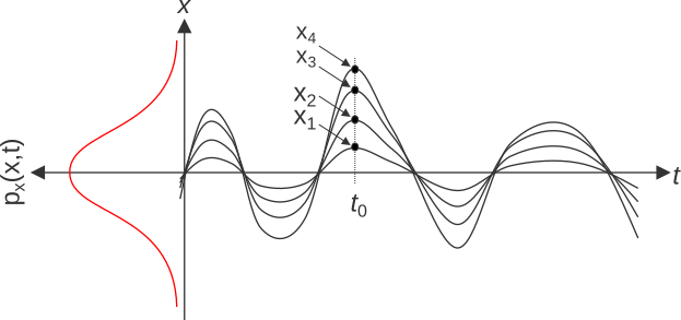
The fluctuations of a physical quantity such as the carrier velocity for example can be described by a random or stochastic process. A random process or stochastic process can be defined as a family of function \(x(t)\), where \(x(t=t_0)\) is a random variable which has a 1st-order probability density function (PDF) \(p_x(x,t)\). The instantaneous value that the random signal will take at a given time \(t_0\) can therefore not be predicted because it can take various values according to the PDF. As it is often the case, this PDF can be assumed to be a Gaussian distribution with zero mean value as shown on the left axis in Figure 1.
3.2.1 Mean value and autocorrelation function
The mean value or expected value \(m_x(t)\) is obtained by averaging the amplitude \(x\) at a given time \(t\) over all possible values [1] \[\begin{equation}\label{eqn:mean_def} m_x(t) = E[x(t)] \triangleq \int\limits_{-\infty}^{+\infty} x \cdot p_x(x,t)\cdot dx. \end{equation}\] Note that in general \(m_x(t)\) is a function of time since \(p_x(x,t)\) depends on time.
The autocorrelation function (ACF) evaluates the statistical dependency between two instantaneous values taken at two different times \(t_1\) and \(t_2\) [1] \[\begin{equation}\label{eqn:autocorrelation_def} R_x(t_1,t_2) =E[x(t_1) x(t_2)] \triangleq \iint\limits_{-\infty}^{\quad+\infty} x_1 \cdot x_2 \cdot p_x(x_1,x_2,t_1,t_2) \cdot dx_1 dx_2, \end{equation}\] where \(x_1 = x(t_1)\) and \(x_2=x(t_2)\). \(p_x(x_1,x_2,t_1,t_2)\) is the 2nd-order distribution function of the process \(x(t)\).
The autocovariance is defined as [1] \[\begin{equation}\label{eqn:covariance_def} C_x(t_1,t_2) = E[(x(t_1)-m_x(t_1)) (x(t_2)-m_x(t_2))] = R_x(t_1,t_2) - m_x(t_1) m_x(t_2). \end{equation}\] From \(\eqref{eqn:covariance_def}\), we see that if either \(m_x(t_1)\) or \(m_x(t_2)\) or both are zero, then \(C_x(t_1,t_2) = R_x(t_1,t_2)\).
The random process is said to be stationary in the wide sense if its mean value is constant and its autocorrelation function only depends on the time difference \(\tau = t_2 - t_1\) [1] \[\begin{align} m_x &=\text{constant},\\ R_x(t_1,t_2) &= R_x(\tau),\\ C_x(t_1,t_2) &= C_x(\tau) = R_x(\tau) - m_x^2. \end{align}\]
Note again that \(C_x(\tau) = R_x(\tau)\) for \(m_x=0\). The normalized autocovariance function (or correlation coefficient) is defined as \[\begin{equation} \rho_x(\tau) = \frac{C_x(\tau)}{\sigma_x^2}, \end{equation}\] where \(\sigma_x^2 = C_x(0)\) is the variance.
It can be shown that for a real process, \(R_x(\tau)\) and \(C_x(\tau)\) are even functions [1] \[\begin{align} R_x(-\tau) &= R_x(\tau),\\ C_x(-\tau) &= C_x(\tau), \end{align}\] and have the following properties [1] \[\begin{align} C_x(0) &= \sigma_x^2,\\ R_x(0) &= \sigma_x^2 - m_x^2,\\ \rho_x(0) &= 1. \end{align}\]
Note that in most of the cases in electronic circuits operating in continuous-time (as opposed to sampled-data systems), the noise sources can be assumed to be stationary. We will see below that it is actually not the case in sampled-data systems where the ACF becomes periodical. We then talk about cyclostationary random process [2], [3] [4] [5]. However, considering the average of the ACF over one period makes it stationary [2] [3] [4] [5].
Additionally, a process is said ergodic when the time averages are equal to the ensemble averages [1] \[\begin{align} \overline{x} &= \lim_{T\rightarrow\infty} \frac{1}{T} \cdot \int\limits_0^T x(t) \cdot dt = E[x] = m_x\\ \overline{x^2} &= \lim_{T\rightarrow\infty} \frac{1}{T} \cdot \int\limits_0^T x^2(t) \cdot dt = E[x^2] = R_x(0). \end{align}\] The conditions for a random process to be ergodic are quite tricky to establish and we will therefore not use this property.
3.2.2 Power spectral density (PSD)
Most of the time, the stationary random process is described in the frequency domain using its power spectral density (PSD). The Wiener-Kintchine theorem theorem states that the PSD of a stationary random process is the Fourier transform of its ACF [1] \[\begin{equation} S_x(f) = \mathcal{F}\left\{R_x(\tau)\right\} = \int\limits_{-\infty}^{+\infty} R_x(\tau)\,e^{-j2\pi f \tau}\,d\tau. \end{equation}\] Note that here we are using the bilateral Fourier transform which makes the pair of transforms symmetrical. We can easily convert the bilateral Fourier transform \(S_x(f)\) back to the unilateral Fourier transform \(S_x^+(f)\) using the following relations \[\begin{align} S_x^+ = \begin{cases} 2S_x(f) & \text{for $f>0$}\\ S_x(f) & \text{for $f=0$}\\ 0 & \text{for $f<0$}. \end{cases} \end{align}\]
Knowing the process PSD, we can find the ACF using the inverse Fourier transform \[\begin{equation} R_x(f) = \mathcal{F}^{-1}\left\{S_x(\tau)\right\} = \int\limits_{-\infty}^{+\infty} S_x(f)\,e^{+j2\pi f \tau}\,df. \end{equation}\]
Despite the PSD is the power per unit bandwidth, its unit is \(V^2/Hz\) for a voltage fluctuation and \(A^2/Hz\) for a current fluctuation. The power then depends on the resistance in which it is dissipated.
3.2.3 Noise power
Sometimes we are more interested in the integrated noise power \(P_x\) rather than its spectral distribution which is then given by integrating the PSD over frequency \[\begin{equation} P_x = \int\limits_{-\infty}^{+\infty} S_x(f) \cdot df = R_x(0). \end{equation}\] The total noise power corresponds to the square of the rms value \[\begin{equation} V_{n,rms}^2 = \int\limits_{-\infty}^{+\infty} S_{v_n}(f) \cdot df = \int\limits_0^{+\infty} S^+_{v_n}(f) \cdot df \end{equation}\] for a noise voltage source and \[\begin{equation} I_{n,rms}^2 = \int\limits_{-\infty}^{+\infty} S_{i_n}(f) \cdot df = \int\limits_0^{+\infty} S^+_{i_n}(f) \cdot df \end{equation}\] for a noise current source.
3.2.4 Sum of two random processes
In the case of two differently jointly stationary processes \(x(t)\) and \(y(t)\) we can define their cross-correlation function (CCF) and cross-covariance by \[\begin{align} R_{xy}(\tau) &= E[x(t+\tau) y(t)],\\ C_{xy}(\tau) &= E[(x(t+\tau)-m_x) (y(t)-m_y)] = R_{xy}(\tau) - m_x\,m_y. \end{align}\]
The normalized cross-covariance is defined as \[\begin{equation} \rho_{xy}(\tau) = \frac{C_{xy}(\tau)}{\sigma_x \cdot \sigma_y}. \end{equation}\]
Two processes \(x(t)\) and \(y(t)\) are uncorrelated if \(C_{xy}(\tau) = 0\) (or \(\rho_{xy}(\tau) = 0\)).
We can also define a cross-power spectral density as the Fourrier transform of its cross-correlation function \[\begin{equation} S_{xy}(f) = \int\limits_{-\infty}^{+\infty} R_{xy}(\tau)e^{-j2\pi f \tau}\,d\tau. \end{equation}\]
If \(z(t) = x(t) + y(t)\) is the sum of two real stationary processes, then its ACF is given by \[\begin{equation} R_z(\tau) = R_x(\tau) + R_y(\tau) + R_{xy}(\tau) + R_{yx}(\tau). \end{equation}\]
In case processes \(x(t)\) and \(y(t)\) are uncorrelated, then \(C_{xy}(\tau) = C_{yx}(\tau) = 0\) and hence \(R_{xy}(\tau) = R_{yx}(\tau) = m_x\,m_y\) which results in \[\begin{equation} R_z(\tau) = R_x(\tau) + R_y(\tau) + 2m_x\,m_y. \end{equation}\]
If in addition \(m_x = 0\) or \(m_y = 0\) (or both), then \[\begin{equation} R_z(\tau) = R_x(\tau) + R_y(\tau). \end{equation}\] This shows that the ACF of the sum of two stationary processes is equal to the sum of their ACF only if the two processes are uncorrelated and one of the two mean value or both are equal to zero. In this case the variance of \(z(t)\) is given by \[\begin{equation} R_z(0) = \sigma_z^2 = R_x(0) + R_y(0) = \sigma_x^2 + \sigma_y^2. \end{equation}\]
In case processes \(x(t)\) and \(y(t)\) are correlated and \(m_x = 0\) or \(m_y = 0\) (or both), then the variance is given by \[\begin{equation} \sigma_z^2 = \sigma_x^2 + \sigma_y^2 + 2c \sigma_x \sigma_y, \end{equation}\] where \(c = \rho_{xy}(0) = \rho_{yx}(0)\) is the correlation coefficient.
In most circuit, the noise sources can be assumed to be statistically independent which implies that they are uncorrelated. There are a few examples where correlation needs to be accounted for. For example in radio-frequency (RF) circuits several noise sources are modeled by two equivalent input-referred noise sources: one shunt current noise and one series voltage noise. Since these two noise sources model the same physical noise sources inside the amplifier, they are usually correlated. Another example is the induced gate current that is produced by the capacitive coupling of the thermal noise voltage fluctuations within the channel of a MOSFET. This induced gate noise is modeled as a shunt current source at the gate terminal whereas the drain current fluctuations due to the thermal noise in the channel is modeled by a current source between drain and source. These two noise current sources are obviously correlated because they originate from the same physical noise in the channel.
3.2.5 Noise in linear systems
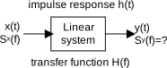
If a stationary random signal \(x(t)\), having a PSD \(S_x(f)\), is applied at the input of a linear system as shown in Figure 2, its output \(y(t)\) is also a stationary random process having a PSD given by \[\begin{equation}\label{eqn:psd_linear_system} \boxed{S_y(f) = |H(f)|^2 \cdot S_x(f)}, \end{equation}\] where \(H(f)\) is the transfer function of the linear system. The linear system could for example be a filter which shapes the input noise according to the square magnitude of its transfer function (phase does not play a role in this case). If the input is a white noise with a constant PSD \(S_x(f) = S_0\), the output PSD is then proportional to the square magnitude of the filter transfer function.
3.2.6 White noise
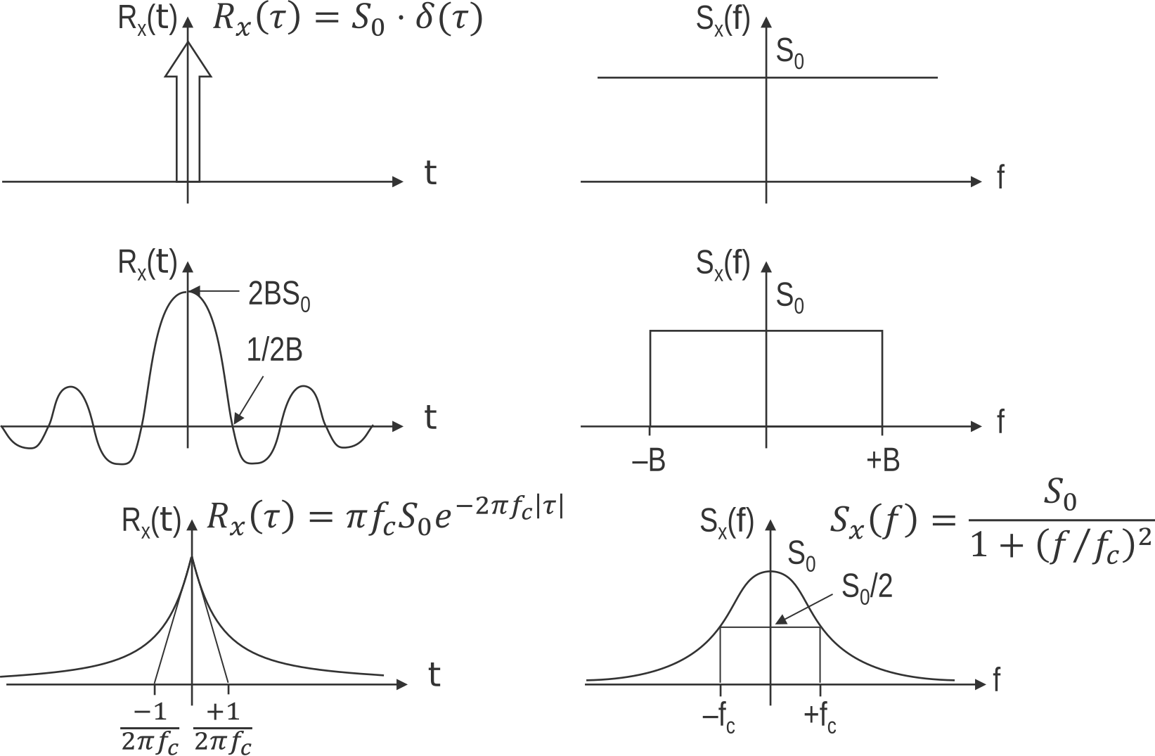
A noise that has a constant PSD, say \(S_0\), as shown in Figure 3 is called white noise. The corresponding ACF is then a simple Dirac impulse function at \(f=0\) with an area \(S_0\). This means that two samples taken with a time difference \(\tau > 0\) are not correlated. White noise is always band-limited in order to maintain a finite power. If the bandwidth limitation is imposed by an ideal low-pass filter as shown in Figure 3, the noise power is then equal to \(P_x = 2B \cdot S_0\). The corresponding ACF then spreads out and becomes \[\begin{equation} R_x(\tau) = 2 S_0 \, \textrm{sinc}(2\pi B \tau) \end{equation}\] where \[\begin{equation} \textrm{sinc}(x) \triangleq \frac{\sin(x)}{x} \end{equation}\] is the sinus cardinal function. It has a first zero at \(\tau = 1/(2B)\) and its value at \(\tau = 0\), \(R_x(0) = 2BS_0\), corresponds to the white noise power (or variance in case the mean value is equal to zero like it is most often the case).
A more realistic case that will be used on many occasions in this book, is the 1st-order low-pass filtered white noise with a cut-off frequency \(f_c\). The PSD then looks like a “Napoleon hat” with \(S_x(f=0) = S_0\) and \(S(f=f_c) = S_0/2\). The corresponding ACF is shown on the bottom left of Figure 3 and corresponds to \[\begin{equation} R_x(\tau) = \pi f_c S_0 \, e^{-2\pi f_c|\tau|}. \end{equation}\] The ACF means that samples taken at two times distant by \(\tau < 1/(2\pi f_c)\) will be correlated whereas they are uncorrelated if \(\tau > 1/(2\pi f_c)\).
3.2.7 Flicker or \(1/f\) noise
Another type of PSD found in many semiconductor devices is flicker noise or 1/f noise. As its name states, this noise has a PSD inversely proportional to frequency \[\begin{equation} S_{1/f}(f) = \frac{K}{|f|^\alpha}, \end{equation}\] where the exponent \(\alpha\) is close to one and \(K\) is a constant. The power (or variance) in a bandwidth limited by \(f_\ell\) at low frequency and \(f_h\) at high frequency assuming \(\alpha = 1\) is given by \[\begin{equation} \sigma_{1/f}^2 = 2 \int\limits_{f_\ell}^{f_h} \frac{K}{f} \cdot df =2K \cdot \ln\left(\frac{f_h}{f_\ell}\right). \end{equation}\] We see that the flicker noise variance increases only with the logarithm of the cut-off frequency \(f_h\) whereas the variance of the white noise is proportional to the cut-off frequency \(f_h\). We also see that the variance of the flicker noise tends to infinity as \(f_h \rightarrow \infty\) or \(f_\ell \rightarrow 0\). The divergence of the flicker noise variance at high frequency does not raise any problem since it is always low-pass filtered. However, the divergence of the flicker noise variance when \(f_\ell \rightarrow 0\) causes many controversies and interrogations. The “problem” of the divergence of the variance when \(f_\ell \rightarrow 0\) can be explained by considering the process as non-stationary and decomposing its ACF into two parts [6] \[\begin{equation} R_{1/f}(t_2,\tau) \approx f(t_2) + f(\tau) \end{equation}\] for \(0 < \tau \ll t_2\) where \(t_2\) is the age of the process and \(\tau = t_2-t_1\). The corresponding PSD follows a \(1/f\) law down to frequency corresponding to the observation time \(T_{obs}\) which is independent of the values of \(t_2\) and \(T_{obs}\) [6].
Flicker noise has been observed as fluctuations not only in semiconductor and electronic devices but in many very different systems, for example [6]: the average seasonal temperature, the annual amount of rainfall, the rate of traffic flow, economic data, the loudness and pitch of music, etc…
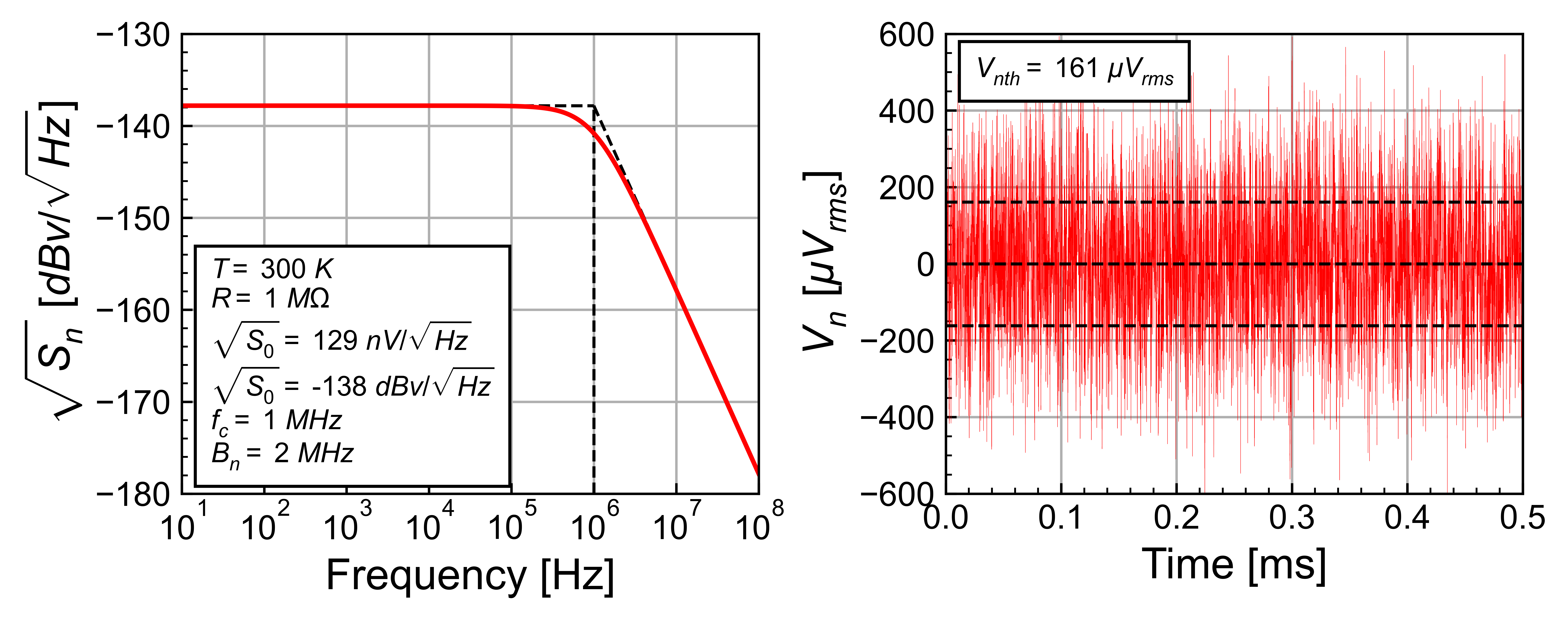
The left plot in Figure 4 shows the square root of the PSD of a 1st-order low-pass filtered white noise corresponding to the thermal noise generated by a resistor \(R = 1 M\Omega\) at room temperature with a cut-off frequency \(f_c = 1 MHz\). The left plot in Figure 4 shows one possible occurrence of this white noise in the time domain. The rms noise voltage is equal to \(V_{nth,rms} = 161 \mu V_{rms}\). We see that the time behavior of white noise is showing a very busy signal with a lot of fluctuations.
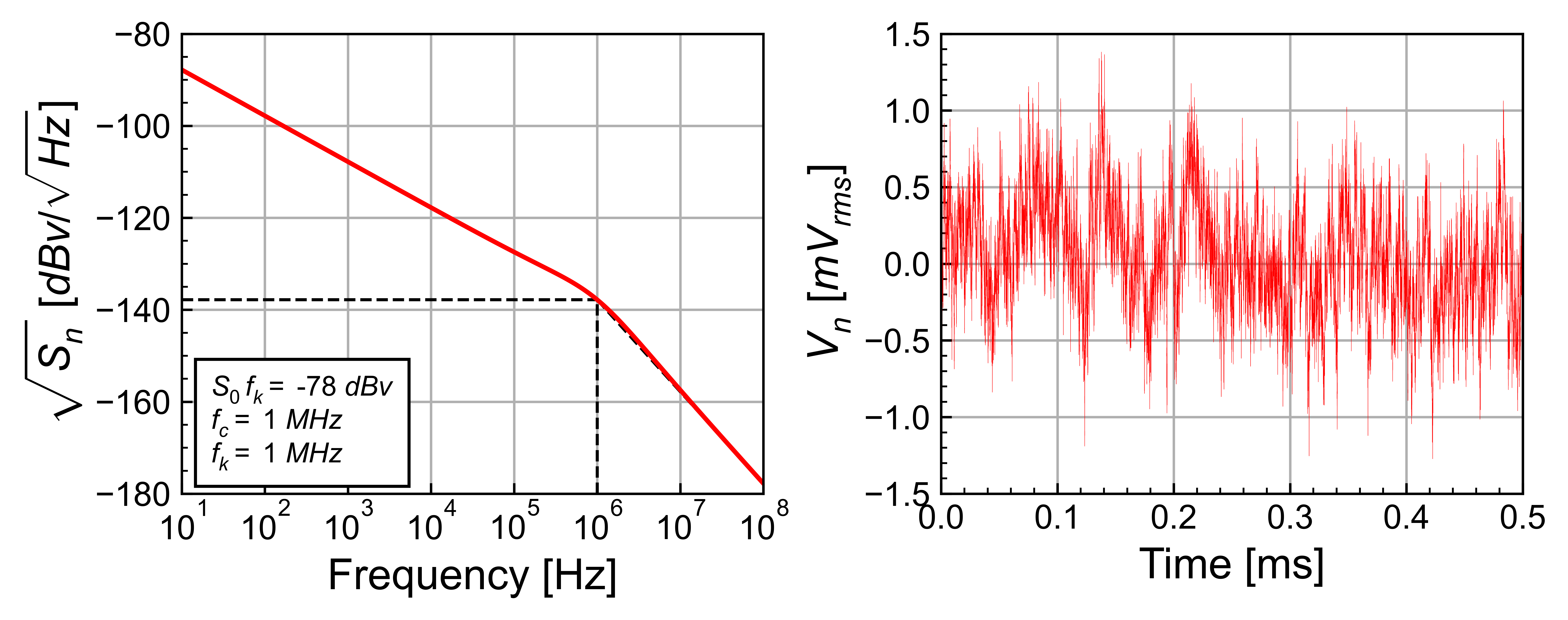
The left plot of Figure 5 shows the square root of the PSD of a 1st-order low-pass filtered flicker noise with the same cut-off frequency \(f_c = 1 MHz\). The right plot shows a possible occurrence of this flicker noise in the time domain. The flicker noise shows the same fast fluctuations although of lesser amplitude on top of a signal that abruptly changes with a large amplitude which is typical of flicker noise.
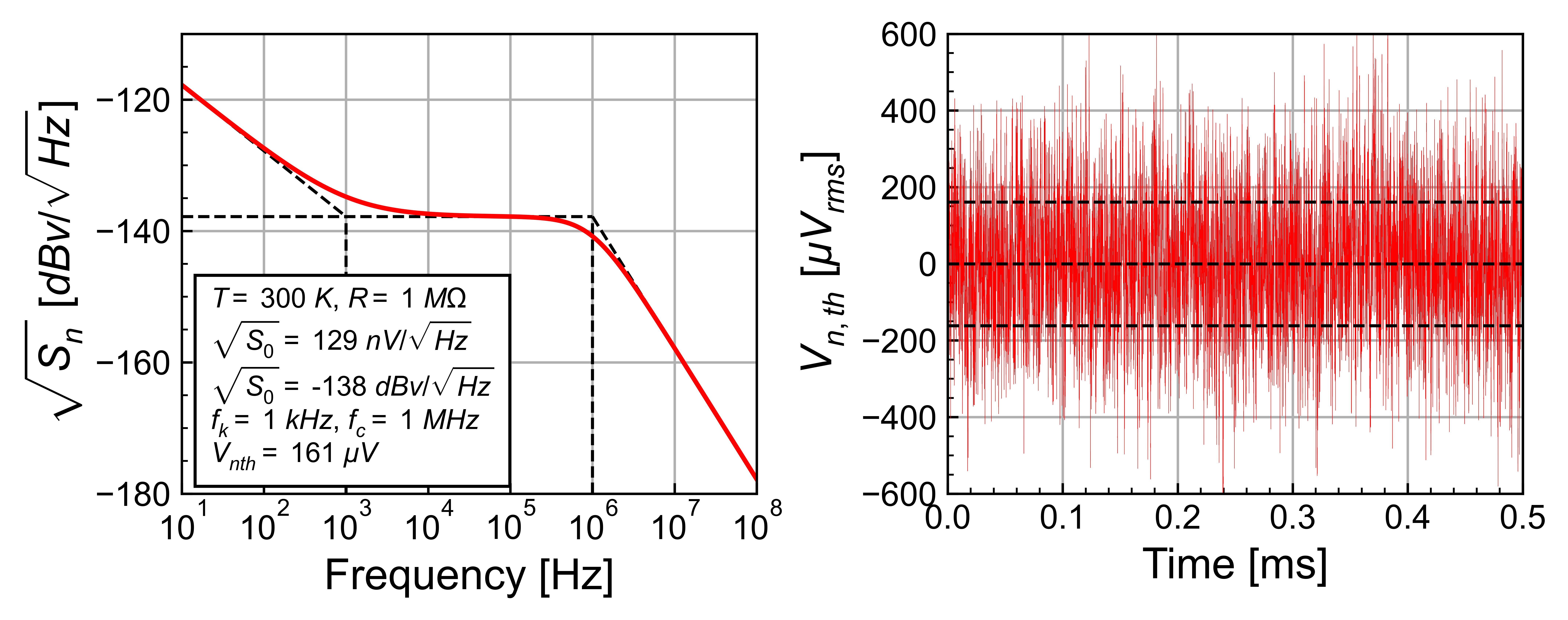
In reality the noise in an amplifier is a superposition of white and flicker noise which are low-pass filtered as shown in the left plot in Figure 6 with a corner frequency \(f_k = 1\,kHz\) and the same cut-off frequency of \(f_c = 1\,Mhz\). When looking at the right plot of Figure 6, we see essentially a similar waveform than for white noise. It is not obvious to recognize the flicker noise component.
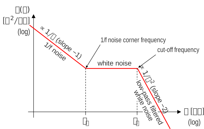
Figure 7 shows the typical PSD that could be seen at the output of an amplifier. The units are in \(V^2/Hz\) and both x- and y-axis are logarithmic. It is made of the low-frequency flicker or \(1/f\) noise showing a slope of \(-1\) (in log-log plot), then a plateau corresponding to the white noise and finally a roll-off inversely proportional to at least \(f^2\) (slope of \(-2\) in this log-log plot) due to poles introducing a low-pass filtering and limiting the bandwidth. The frequency for which the \(1/f\) noise becomes equal to the white noise is called the corner frequency. In advanced CMOS technologies this corner frequency can be very high (typically above 1 MHz) and the noise is dominated by flicker noise for frequencies below \(f_k\). This means that when designing circuits operating at low-frequency, such as sensor interfaces or baseband circuits, in advanced CMOS technologies, the noise is completely dominated by flicker noise. Fortunately, there are techniques to reduce or even eliminate this \(1/f\) noise. The latter will be presented in details in Chapter 8.
3.2.8 Equivalent noise bandwidth
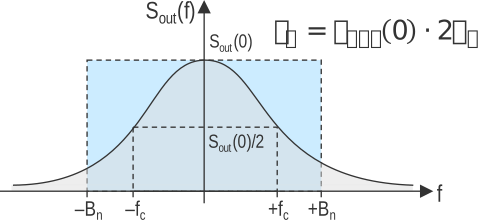
In some application the designer is more interested in the overall noise power rather than the PSD. This means that he needs to integrate the noise PSD over frequency. The concept of equivalent noise bandwidth is introduced to avoid doing this integration over and over again. Let’s assume that we have a white noise PSD that is low-pass filtered as shown in Figure 8. We can define an ideally low-pass filtered white noise that has the same value than \(S_0\) at \(f = 0\) than the low-pass filtered white noise PSD and an equivalent bandwidth \(B_n\) such that the power of both PSDs are equal. This leads to the following definition of the equivalent noise bandwidth \[\begin{equation} B_n = \frac{1}{2 S_{out}(0)} \int\limits_{-\infty}^{+\infty} S_{out}(f) \cdot df = \frac{1}{S_{out}(0)} \int\limits_{0}^{+\infty} S_{out}(f) \cdot df = \frac{P_{out}}{2 S_{out}(0)}. \end{equation}\] If the input noise is a white noise of PSD \(S_0\), the output noise is then given by \[\begin{equation} S_{out}(f) = |H(f)|^2 \cdot S_0 \end{equation}\] and the equivalent noise bandwidth then reads \[\begin{equation}\label{eqn:noise_bandwidth_def} B_n = \frac{1}{2 |H(0)|^2 S_0} \int\limits_{-\infty}^{+\infty} |H(f)|^2 \cdot S_0 \cdot df = \frac{1}{|H(0)|^2} \int\limits_{0}^{+\infty} |H(f)|^2 \cdot df \end{equation}\] which only depends on the square magnitude of the transfer function \(H(f)\). Note that \(|H(0)|\) is the dc gain magnitude. The equivalent noise bandwidth can therefore be calculated ahead of time for various transfer functions. presents the noise bandwidth for the most commonly used transfer functions.
The noise power can then simply be expressed as \[\begin{equation}\label{eqn:V2nout} V_{nout}^2 = S_{out}(0) \cdot B_n = S_0 \cdot |H(0)|^2 \cdot B_n \end{equation}\] which avoids doing any integration. Of course \(\eqref{eqn:V2nout}\) only holds for a white noise input PSD.
| Filter Type | Noise Transfer Function | Noise Bandwidth |
|---|---|---|
| 1st-order LP | \(\frac{1}{1 + \frac{s}{\omega_c}}\) | \(\frac{\omega_c}{4}\) |
| 2nd-order LP | \(\frac{1}{1 + \frac{s}{\omega_0\,Q} + \left(\frac{s}{\omega_0}\right)^2}\) | \(\frac{\omega_0\,Q}{4}\) |
| 2nd-order BP | \(\frac{\frac{s}{\omega_0\,Q}}{1 + \frac{s}{\omega_0\,Q} + \left(\frac{s}{\omega_0}\right)^2}\) | \(\frac{\omega_0}{4 Q}\) |
| 2nd-LP with zero | \(\frac{1 + \frac{s}{\omega_z}}{1 + \frac{s}{\omega_0\,Q} + \left(\frac{s}{\omega_0}\right)^2}\) | \(\frac{\omega_0}{4 Q} \left[1 + \left(\frac{\omega_0}{\omega_z}\right)^2\right]\) |
The definition \(\eqref{eqn:noise_bandwidth_def}\) does not strictly apply to the case of a bandpass filter, because the dc gain \(|H(0)|\) is actually zero. The dc gain should be replaced by the gain at the resonance frequency which in the above case has been set to one.
We can find the equivalent noise bandwidth in the case of a 1st-order low-pass filtered white noise \[\begin{equation} B_n = \int\limits_{0}^{+\infty} \frac{1}{1 + (f/f_c)^2} \cdot df = f_c \cdot \int\limits_{0}^{+\infty} \frac{1}{1 + x^2} \cdot dx = \frac{\pi}{2}\,f_c. \end{equation}\] We see that the equivalent noise bandwidth is \(\pi/2\)-times larger than the cut-off frequency. As shown in Figure 8, this is due to the area below the curve that is above the cut-off frequency \(f_c\) which contributes to additional noise power. The sharper the low-pass filter, the closer the noise bandwidth is to the cut-off frequency. Therefore this factor \(\pi/2\) is a kind of “worse case” situation.
The above definition of the equivalent noise bandwidth applies to white noise only. However in an amplifier we have a combination of a white noise and flicker noise which PSD can be written as \[\begin{equation}\label{eqn:Sn_white_flicker} S_n(f) = S_0 \cdot \left(1 + \frac{f_k}{|f|}\right), \end{equation}\] where \(S_0\) is the white noise component and \(f_k\) the corner frequency (frequency at which the 1/f noise becomes equal to the white noise). The noise power assuming the noise is filtered by a 1st-order low-pass filter having a cut-off frequency \(f_c\) is then given by \[\begin{equation} V_n^2 = 2 \int\limits_{0}^{+\infty} \frac{S_n(f)}{1+(f/f_c)^2} \cdot df. \end{equation}\]
We can then define an equivalent noise bandwidth \(B_n\) that includes the 1/f noise contributionaccording to \[\begin{equation} B_n \triangleq \frac{V_n^2}{2 S_0} = \int\limits_{0}^{+\infty} \frac{1 + f_k/f}{1+(f/f_c)^2} \cdot df = f_c \cdot \int\limits_{0}^{+\infty} \frac{dx}{1+x^2} + f_k \cdot \int\limits_{x_\ell}^{+\infty} \frac{dx}{x(1+x^2)} \end{equation}\] where \(x \triangleq f/f_c\) and \(x_\ell \triangleq f_\ell/f_c\). It is actually convenient to choose \(f_\ell = 1\;Hz\) which results in \[\begin{equation} B_n = \frac{\pi}{2}\,f_c + \frac{f_k}{2}\,\ln\left[1 + \left(\frac{f_c}{f_\ell}\right)^2\right] \cong \frac{\pi}{2}\,f_c + f_k\,\ln\left(\frac{f_c}{1\,Hz}\right). \end{equation}\] We see that the contribution of the 1/f noise to the total noise power is scaling only with the logarithm of \(f_c\), whereas the white noise contribution is proportional to \(f_c\).
3.3 The main noise sources in electronic devices
There are mainly three kinds of noise sources in electronic devices:
1. Thermal noise:
- Due to the thermal excitation of charge carriers.
- PSD proportional to absolute temperature.
- Appears as white noise PSD.
2. Shot Noise:
- Due to carriers randomly crossing a potential barrier.
- Depends on dc bias current.
- Appears as white noise PSD.
3. Flicker Noise:
- Due to traps in semiconductors.
- Has a 1/f PSD.
- Significant in MOS transistors at low frequencies.
Each of the above noise sources are discussed in more details below.
3.3.1 Thermal noise
3.3.1.1 The equipartition theorem
Thermal noise is related to the thermal agitation of carriers and is therefore directly linked to the equipartition theorem [7]. The latter states:
every closed physical system at temperature \(T\) contains energy of average amount \(k_B\,T/2\) per degree of freedom, where \(k_B = 1.38 \times 10^{-23}\,J\) is the Boltzmann constant.
We can illustrate this statement with the following experiment. Consider a gaz of electrons having a Maxwellian velocity distribution given by [7] \[\begin{equation} p(v) = \sqrt{\frac{m}{2 \pi k_B\,T}} \cdot e^{-\frac{m v^2}{2 k_B\,T}}, \end{equation}\] where \(p(v) \cdot dv\) represents the the probability of finding one electron having a velocity comprised between \(v\) and \(v + dv\). The average energy of the electron at equilibrium is then given by \[\begin{equation} \overline{W} = E\left[m \frac{v^2}{2}\right] = \frac{m}{2} \, E\left[v^2\right] = \frac{m}{2} \cdot \int\limits_0^{+\infty} v^2 \cdot p(v) \cdot dv = \frac{k_B\,T}{2}. \end{equation}\] Hence for a one degree of freedom system we have [7] \[\begin{equation} \frac{m \overline{v^2}}{2} = \frac{k_B\,T}{2}. \end{equation}\]
3.3.1.2 The Nyquist theorem - Microscopic derivation
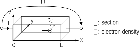
There are several ways to derive the famous Nyquist theorem for thermal noise which states that the PSD of the voltage fluctuation across a piece of conductor having a resistance \(R\) is simply \(S_n = 4 k_B\,T R\). Nyquist originally derived this formula from a consideration using transmission lines [8]. We will derive it following the microcscopic approach proposed by Kittel [7] and later by van der Ziel [9]. Let’s consider a piece of conductive material with a section \(A\) and a length \(L\). The voltage across it is given by Ohm’s law \[\begin{equation} U = R \cdot I = R\,A\,J = R\,A\,n\,q\,v, \end{equation}\] where \(n\) is the electron density and \(v\) is the drift velocity along the x-axis, averaged over the ensemble of electrons \(N = n\,A\,L\) \[\begin{equation} v = \frac{1}{N} \sum_i v_i. \end{equation}\] The voltage \(U\) can then be written as \[\begin{equation} U = \frac{q\,R}{L} \sum_i v_i = \sum_i u_i, \end{equation}\] where \(u_i = q\,R/L v_i\) is the voltage contribution of a single electron. If no dc current is flowing, then \(I = 0\), \(U = 0\) and \(v = 0\). However, despite the average voltage being zero, the variances of the voltage and drift velocity are not \(\overline{v^2} = E[v^2] \neq 0\) and \(\overline{U^2} = E[U^2] \neq 0\). Assuming there is no correlation between electrons, the ACF of \(U\) is given by \[\begin{equation} R_u(\tau) = \sum_i R_{u_i}(\tau) = \left(\frac{q\,R}{L}\right)^2\,\sum_i R_{v_i}(\tau), \end{equation}\] where \(R_{v_i}(\tau)\) is the ACF of the individual electron velocity \(v_i\). Assuming \(v_i\) has a Maxwellian distribution, then \(R_{v_i}(\tau)\) is given by \[\begin{equation} R_{v_i}(\tau) = R_{v_i}(0) \,e^{-\frac{|\tau|}{\tau_0}}, \end{equation}\] where \(\tau_0\) is the relaxation time or the mean time of flight of the conduction electrons. \(R_{v_i}(0)\) can be found by using the equipartition theorem considering the system has only one degree of freedom (namely the motion along the x-axis) according to \[\begin{equation} m\frac{v_i^2}{2} = \frac{m}{2} R_{v_i}(0) = \frac{k_B\,T}{2}, \end{equation}\] which results in \[\begin{equation} R_{v_i}(0) = \frac{k_B\,T}{m}. \end{equation}\] The ACF of the voltage \(U\) then simply writes \[\begin{equation} R_u(\tau) = N\,\left(\frac{q\,R}{L}\right)^2\,\frac{k_B\,T}{m}\,e^{-\frac{|\tau|}{\tau_0}}. \end{equation}\] The corresponding bilateral PSD of the voltage is given by \[\begin{equation}\label{eqn:lorentzian} S_u(f) = N\,\left(\frac{q\,R}{L}\right)^2\,\frac{k_B\,T}{m}\,\frac{2\tau_0}{1 + (2\pi f \tau_0)^2}. \end{equation}\] \(\eqref{eqn:lorentzian}\) is called a *Lorentzian spectrum} which is characterized by a 1st-order low-pass function which passband gain is inversely proportional to its cut-off frequency.
Usually in conductors such as metals \(\tau_0 < 10^{-13}\,s\) and hence we can consider that \(2\pi f \tau_0 \ll 1\). \(\eqref{eqn:lorentzian}\) then becomes \[\begin{equation}\label{eqn:Su2} S_u(f) \cong N\,\left(\frac{q\,R}{L}\right)^2\,\frac{k_B\,T}{m}\,2\tau_0 = 2 k_B\,T\,R\cdot\frac{n\,A\,q^2\,R\,\tau_0}{m\,L}. \end{equation}\] Recalling that the conductivity \(\sigma\) is given by \(\sigma = q\,\mu\,n\) and the mobility \(\mu\) by \(\mu = q\,\tau_0/m\), the resistance can then be written as \[\begin{equation}\label{eqn:R_thermal_noise} R = \frac{L}{\sigma\,A} = \frac{L}{A}\,\frac{m}{q^2\,n\,\tau_0}. \end{equation}\] The second term of \(\eqref{eqn:Su2}\) becomes unity after replacing \(R\) by \(\eqref{eqn:R_thermal_noise}\) which leads to the bilateral PSD of thermal noise \[\begin{equation} S_u(f) = 2 k_B\,T\,R\quad\mathrm{(bilateral)}, \end{equation}\] or in the more conventional unilateral form \[\begin{equation}\label{eqn:fourktR} \boxed{S_u^+(f) = 4\,k_B\,T\,R.} \end{equation}\]
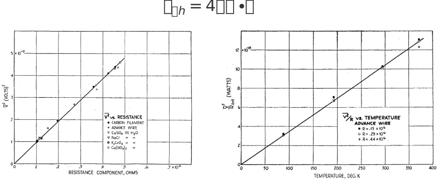
Figure 10 shows the original measurements made by Johnson and published in 1928 [10]. The left plot demonstrates the proportionality between the noise voltage PSD and the resistance measured for different conductive materials. The right plot validates the proportionality of the PSD with the absolute temperature.
3.3.1.3 The Nyquist theorem - Thermal noise of a passive RLC network
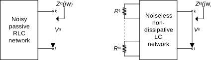
The Nyquist theorem can be extended to the case shown in Figure 11. It can be shown that the PSD of the noise voltage at a given port of a passive RLC network due to the thermal noise generated by the resistors in this passive network is given by \[\begin{equation} S_{V_n}(f) = 4 k_B\,T \cdot \Re\{Z(j2\pi f)\}, \end{equation}\] where \(Z(j2\pi f)\) is the impedance that is seen when looking into this port.
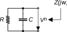
The generalized Nyquist theorem can be illustrated with the simple 1st-order low-pass filter shown in Figure 12. The impedance seen when looking into the port is given by \[\begin{equation} Z(j\,\omega) = \frac{1}{1/R + j\omega C} = \frac{R}{1 + j\,\omega R C} = \frac{R}{1 + (\omega R C)^2} -j\,\frac{\omega R^2 C}{1 + (\omega R C)^2}, \end{equation}\] from which we derive the noise voltage PSD as \[\begin{equation} S_{V_n}(f) = 4 k_B\,T \cdot \Re\{Z(j2\pi f)\} = \frac{4 k_B\,T\,R}{1 + (2\pi f RC)^2}. \end{equation}\]
3.3.1.4 \(k\,T/C\) noise
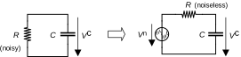
Consider the 1st-order low-pass filter shown in Figure 13. The noisy resistor can be modeled by a noiseless resistor in series with a noise voltage source having a PSD equal to \(4 k_B\,T R\). Using \(\eqref{eqn:psd_linear_system}\), we can calculate the PSD of the voltage across the capacitor \(C\) \[\begin{equation} S_{V_c}(f) = \frac{4 k_B\,T\,R}{1 + (2 \pi f \tau)^2}, \end{equation}\] where \(\tau = RC\). The variance of the voltage across the capacitor is then given by \[\begin{equation}\label{eqn:kT_over_C} V_c^2 = 4 k_B\,T\,R\, \int\limits_0^{+\infty} \frac{df}{1 + (2 \pi f \tau)^2} = 4 k_B\,T\,R\,B_n = 4 k_B\,T\,R\,\frac{\pi}{2}\,\frac{1}{2\pi\,R C} = \frac{k_B\,T}{C}. \end{equation}\] The noise voltage variance is inversely proportional to the capacitance and independent of the resistance \(R\). The reason is simply because the noise PSD level is proportional to \(R\), whereas the equivalent noise bandwidth \(B_n\) is inversely proportional to \(R\), making its product independent of \(R\).
This result can be obtained directly without integration by applying the equipartition theorem. The average stored energy on the capacitor \(C\) is \(\overline{W} = C\,\overline{V_c^2}/2\). Since the resistor and capacitor are in thermal equilibrium and there is only one degree of freedom (the voltage across the capacitor), applying the equipartition theorem results in \(\overline{W} = k_B\,T/2\). Equating the two results gives \(C\,\overline{V_c^2} = k_B\,T\) and finally \(\eqref{eqn:kT_over_C}\) [11].
So we get \(kT/C\) noise when the noise and the equivalent noise bandwidth are both set by the same resistance or transconductance. If the thermal noise and the noise bandwidth are decoupled, we still get \(kT/C\) noise but the \(C\) is usually a more complex expression which may for example involve several capacitances and capacitance ratioes and eventually a \(G_m\,R\) product.
Is the \(k\,T/C\) a hard lower limit or can we find circuits that break this limit?
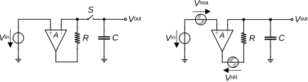
The \(k\,T/C\) is indeed a lower limit for passive RLC circuits. However, introducing active circuits can lower this limit. An example of a circuit that breaks the \(k\,T/C\) limit is shown in Figure 14. This circuit is actually a simple sample-and-hold stage (S&H). Assuming and ideal OPAMP, when the switch is closed the input voltage is reproduced across the hold capacitor \(C\). When the switch is opened this voltage is sampled on \(C\) together with the noise generated by the resistor and the OPAMP. If the voltage amplifier is considered as ideal (infinite input impedance, infinite bandwidth, but finite gain \(A\)), when the switch is closed, the capacitor sees an equivalent resistance \(R_{eq} = R/(A + 1)\). The noise bandwidth is therefore made \(A + 1\) times larger compared to that without the amplifier. Assuming first that the amplifier is noiseless, the noise voltage across the capacitor due to the thermal noise of the resistor only is \[\begin{equation} S_{V_n}(f) = 4 k_B\,T\,R \cdot \frac{1}{(A + 1)^2} \cdot \frac{1}{1 + (f/f_c)^2}. \end{equation}\] with \(f_c = (A + 1)/(2 \pi\,R\,C)\). The thermal noise level below \(f_c\) is inversely proportional to \((A + 1)^2\), whereas the noise bandwidth is proportional to \(A + 1\) resulting in a variance of the noise voltage across \(C\) that is inversely proportional to \(A + 1\) \[\begin{equation} V_n^2 = 4 k_B\,T\,R \cdot \frac{1}{(A + 1)^2} \cdot \frac{A + 1}{4 R\,C} = \frac{k_B\,T}{C} \cdot \frac{1}{A + 1} = \frac{\gamma_{neq}\,k_B\,T}{C}, \end{equation}\] where the noise excess factor \(\gamma_{neq} = 1/(A + 1)\) can be made smaller than 1 thanks to the voltage gain of the noiseless amplifier.
If the input-referred thermal noise resistance of the amplifier \(R_{noa}\) is accounted for, the noise excess factor then writes \[\begin{equation} \gamma_{neq} = \frac{A^2\,R_{noa}/R + 1}{A + 1}. \end{equation}\] The noise excess factor can still be made smaller than one if the input-referred thermal noise resistance of the amplifier \(R_{noa}\) is \(A^2\) smaller than \(R\).
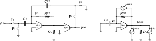
A practical example of a sub-\(k T/C\) noise circuit is the sample-and-hold (S&H) circuit shown in Figure 15 [12]. The circuit operates as follows: the input voltage is sampled on capacitor \(C_S\) at the end of phase \(\Phi_1\) while capacitor \(C_{FB}\) is discharged. At the same time the noise on \(C_S\) is also sampled and transferred to the feedback capacitor during phase \(\Phi_2\). We can calculate the noise voltage across capacitor \(C_S\) during phase \(\Phi_1\) using the circuit shown on the right of Figure 15 accounting for the three thermal noise sources, namely the noise from the two resistors \(R_{FB}\) and \(R_L\) modelled by current sources \(I_{nR_{FB}}\) and \(I_{nR_L}\) and of the transconductor modelled by current source \(I_{nG_m}\). The cut-off frequency is given by \[\begin{equation} \omega_c = \frac{G_{m1} R_L + 1}{C_S\,(R_{FB} + R_L)}, \end{equation}\] while the PSD of \(V_n\) below the cut-off frequency is given by \[\begin{equation} S_{V_n} = 4 k_B\,T \cdot R_n, \end{equation}\] with \[\begin{equation} R_n = \frac{R_{FB}+R_L(1+\gamma_n G_{m1} R_L)}{(G_{m1} R_L + 1)^2}. \end{equation}\] Since the noise on capacitor \(C_S\) is filtered by a 1st-order low-pass filter, we can calculated the noise power using the equivalent noise bandwidth \(B_n=\omega_c/4\) resulting in \[\begin{equation}\label{eqn:V2n_sub_kT_over_C} V_n^2 = \frac{k_B\,T}{C_S} \cdot \frac{R_{FB}/R_L + \gamma_n\,G_{m1} R_L + 1}{(R_{FB}/R_L + 1)(G_{m1} R_L + 1)}. \end{equation}\] We see that removing the transconductor (i.e. setting \(G_{m1} = 0\)), reduces the circuit to a passive circuit where the resistance that sets at the same time the cut-off frequency and the thermal noise level is the series connection of \(R_{FB}\) and \(R_L\) and leads to a noise power equal to \(k_B\,T/C_S\). Introducing the transconductor allows to extend the cut-off frequency by a factor \(G_{m1} R_L + 1\) while the noise level is roughly divided by \((G_{m1} R_L + 1)^2\), leading to a noise power that is roughly divided by \(G_{m1} R_L + 1\) as shown by \(\eqref{eqn:V2n_sub_kT_over_C}\). For \(R_{FB}/R_L \gg \gamma_n\,G_{m1}\,R_L \gg 1\), \(\eqref{eqn:V2n_sub_kT_over_C}\) reduces to \[\begin{equation} V_n^2 \cong \frac{k_B\,T}{C_S} \cdot \frac{1}{G_{m1} R_L}, \end{equation}\] which ideally can be made arbitrarily small by making \(G_{m1} R_L\) sufficiently large.
It is shown in [12]} that the rms noise voltage could be reduced from \(V_{n,rms} = 72\,\mu V_{rms}\) for the conventional sampling down to \(V_{n,rms} = 52\,\mu V_{rms}\) when the feedback circuit is activated. This corresponds to a 48% or 2.8,dB reduction in power.
3.3.1.5 The Bode theorem
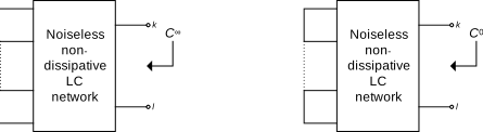
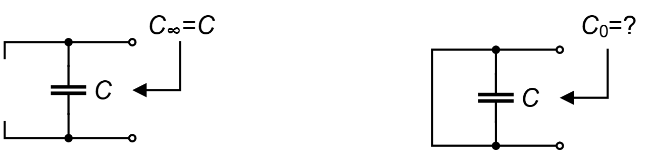
It can be shown that the variance of the thermal noise voltage \(V_n\) at a port of a passive RLC network can be obtained without computing any integral by using the Bode theorem stating [13] \[\begin{equation}\label{eqn:Bode_th} \overline{V_n^2} = k_B\,T \, \left(\frac{1}{C_\infty} - \frac{1}{C_0}\right), \end{equation}\] where \[\begin{equation} \frac{1}{C_\infty} = \lim_{s \rightarrow \infty} [s \cdot Z(s)] \end{equation}\] and \[\begin{equation} \frac{1}{C_0} = \lim_{s \rightarrow 0} [s \cdot Z(s)]. \end{equation}\] \(C_\infty\) actually corresponds to the capacitance that is seen when looking into the port after having removed all the resistors, whereas \(C_0\) is the capacitance seen when looking into the port after having replaced all the resistors with short-circuits. The thermal noise variance in passive circuits can therefore be calculated at any port just by circuit inspection only without performing any cumbersome integration! However, the Bode theorem only applies to passive circuits. We will see later that it can be used for an approximate calculation of the thermal noise variance in switched-capacitor circuits as described in Chapter~10.
We can illustrate the Bode theorem with the simple 1st-order low-pass filter shown in Figure 17. The capacitance seen across \(C\) after having removed resistor \(R\) is simply \(C_\infty = C\). The capacitance seen after replacing \(R\) with a short-circuit is a bit more tricky to evaluate. What is the capacitance of a short-circuit? We actually can apply the more formal definition \[\begin{equation} \frac{1}{C_0} = \lim_{s \rightarrow 0} [s \cdot Z(s)] = \lim_{s \rightarrow 0} \frac{sR}{1 + sRC} = 0 \end{equation}\] and hence \(C_0 = \infty\). Replacing the values of \(C_\infty\) and \(C_0\) in \(\eqref{eqn:Bode_th}\) results in the expression found earlier in \(\eqref{eqn:kT_over_C}\).
3.3.2 Shot noise
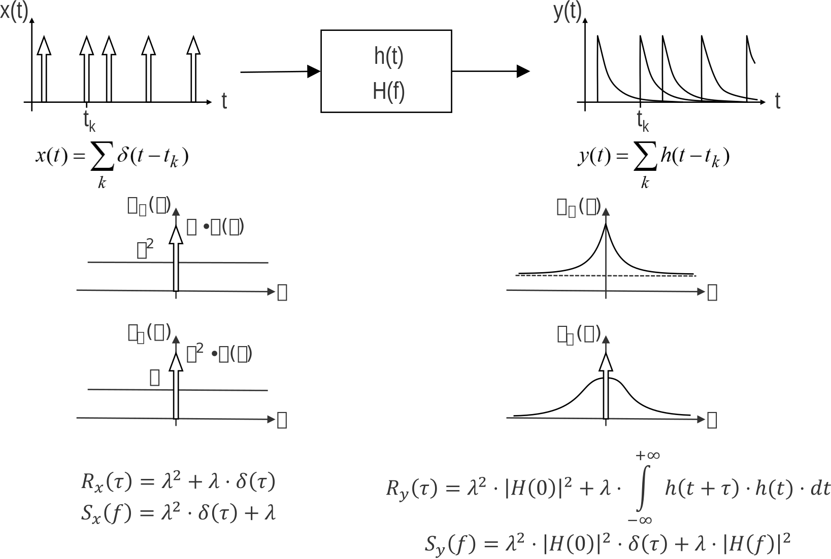
Shot noise is tightly linked to the Poisson process which is characterized by a sequence of independent random events, occurring at any time \(t_k\) with the same probability as shown in Figure 18. The probability to have exactly \(n\) events in the time interval \([0,t]\) is given by [1] \[\begin{equation} p_n(t) = \frac{(\lambda \cdot t)^n}{n!} \cdot e^{-\lambda \cdot t}, \end{equation}\] where \(\lambda\) is the average number of events per seconds, which can be assumed to be constant. The average (or expected) number of events therefore grows linearly with time \[\begin{equation} E[n] = \sum_{n=0}^{+\infty} n \cdot p_n(t) = \lambda \cdot t. \end{equation}\]
The shot noise process is defined by a sequence of pulses according to [1] \[\begin{equation} y(t) = \sum_k h(t -t_k), \end{equation}\] where \(t_k\) are random points in time following a Poisson process with uniform density \(\lambda\). The random signal \(y(t)\) can be considered as the output of a linear system having an impulse response \(h(t)\) and a sequence of Poisson impulses at the input [1] \[\begin{equation} x(t) = \sum_k \delta(t-t_k). \end{equation}\] It can be shown that the PSD of process \(x(t)\) is made of a DC component \(\lambda^2 \cdot \delta(f)\) and an additional white noise \(\lambda\) as shown in Figure 18 [1] \[\begin{equation}\label{eqn:shot_noise_input_psd} S_x(f) = \lambda^2 \cdot \delta(f) + \lambda. \end{equation}\] \(\eqref{eqn:shot_noise_input_psd}\) shows the fundamental relation of shot noise where the level of the white noise resulting from the fluctuations of the events in time is equal to the average number of events per second. The PSD of the process \(y(t)\) is then given by \[\begin{equation} S_y(f) = \lambda^2 \cdot |H(0)|^2 \cdot \delta(f) + \lambda \cdot |H(f)|^2, \end{equation}\] where \(|H(0)|\) is the DC gain of the system.
3.3.2.1 Shot noise in a p-n junction

The above description of the shot noise process can be used to describe the fluctuations of the current passing through a p-n junction. It is well-known that the dc current through a p-n junction is given by the junction law \[\begin{equation} I_d = I_s \cdot \left[e^{\frac{V}{U_T}} - 1\right], \end{equation}\] where \(I_s\) is the saturation current. The current \(I_d\) is composed of the current \(I_d + I_s = I_s \cdot e^{\frac{V}{U_T}}\) due to holes injected from the p+ region into the n region and recombining there or reaching the ohmic contact, and the current \(-I_s\) due to holes generated in the n region and collected by the p region.
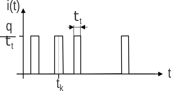
As shown in Figure 19, the current is not constant but fluctuates. If we would be able to zoom in the current versus time waveform as illustrated in Figure 20, we would see that the current is made of individual impulses, each corresponding to the event of a single carrier crossing the potential barrier in one direction or the other. We can consider that the current impulse is a rectangular impulse having a duration \(\tau_t\) corresponding to the transit time through the depletion region of the p-n junction and having an area corresponding to the unit charge \(q\). Assuming that each carrier has the same probability to cross the barrier at any time and that the average number of carrier crossing the barrier per unit time remains constant and equal to \(\lambda\), the current \(i(t)\) is a shot noise process with \[\begin{equation} \lambda \cdot q = (I_d + I_s) + I_s = I_d + 2 I_s = I_{eq}. \end{equation}\] The PSD of the current \(i(t)\) is then given by \[\begin{equation} S_I(f) = (\lambda \cdot q)^2 \cdot \delta(f) + \lambda \cdot q^2 \cdot \textrm{sinc}^2(\pi f \tau_t) = I_{eq}^2 \cdot \delta(f) + I_{eq} \cdot q \cdot \textrm{sinc}^2(\pi f \tau_t). \end{equation}\] The bilateral PSD of the current fluctuation \(\Delta I\) is then given by \[\begin{equation} S_{\Delta I}(f) = I_{eq} \cdot q \cdot \textrm{sinc}^2(\pi f \tau_t) \cong q \cdot I_{eq} = q \cdot (I_d + 2 I_s)\qquad\text{for: } f \ll 1/(\pi \tau_t) \end{equation}\] or in unilateral PSD the well-known expression \[\begin{equation} \boxed{S_{\Delta I} = 2q \cdot I_{eq} \cong 2q \cdot I_d.} \end{equation}\] If we use the simple shot noise expression \(S_{\Delta I} = 2q \cdot I_d\), at \(V=0\) the junction current is \(I_d=0\) but of course the noise PSD cannot be zero. This is why we need to use the full expression with \(I_{eq}\) instead of \(I_d\) which results in \(S_{\Delta I} = 4q \cdot I_s\). We can also express the PSD as if it would be thermal noise which gives the following unilateral PSD \[\begin{equation}\label{eqn:Shot_pn_Sid1} S_{\Delta I} = 2 k_B\,T \cdot G_d \cdot \frac{I_d + 2 I_s}{I_d + I_s} \end{equation}\] where \(G_d\) is the small-signal differential conductance \[\begin{equation} G_d \triangleq \frac{d I_d}{d V_d} = \frac{I_d + I_s}{U_T}. \end{equation}\] For \(V=0\) and \(I_d=0\), the differential conductance becomes \(G_{d0} = I_s/U_T\) and \(\eqref{eqn:Shot_pn_Sid1}\) reduces to the thermal noise expression \(S_{\Delta I} = 4 k_B\,T \cdot G_{d0}\) where \(G_{d0} \triangleq G_d(V_d=0)\). When the pn junction is forward biased then \(I_d \gg I_s\) and \(\eqref{eqn:Shot_pn_Sid1}\) becomes \[\begin{equation}\label{eqn:Shot_pn_Sid2} S_{\Delta I} = 2 k_B\,T \cdot G_d = 2 k_B\,T \cdot \frac{I_d}{U_T} = 2q \cdot I_d. \end{equation}\] Looking at \(\eqref{eqn:Shot_pn_Sid2}\), we sometimes say that shot noise produces “half thermal noise.”
3.3.3 Flicker noise
Flicker noise or 1/f noise is a random process with zero mean value and characterized by its PSD \[\begin{equation} S_{1/f}(f) = \frac{K_f}{|f|^\alpha}, \end{equation}\] with \(\alpha\) close to one and where \(K_f\) is a constant parameter related to the technology. The power or variance in a bandwidth \([f_\ell,f_h]\) assuming \(\alpha = 1\) is given by \[\begin{equation}\label{eqn:flicker_sigma2} \sigma_{1/f}^2 = 2 \int\limits_{f_\ell}^{f_h} \frac{K_f}{f} \cdot df = 2K_f \cdot\ln\left(\frac{f_h}{f_\ell}\right). \end{equation}\] We see from \(\eqref{eqn:flicker_sigma2}\) that the 1/f noise variance tends to infinity for \(f_h \rightarrow \infty\) or \(f_\ell \rightarrow 0\). The divergence of the variance at high frequency does not cause a problem since there is always a bandwidth limitation. However, the divergence of the variance when \(f_\ell \rightarrow 0\) causes many controversies and interrogations! This anomaly can be explained when considering that the 1/f noise is actually a non-stationary process which ACF can be decomposed into the sum of a term that only depends on the process age \(t_2\) and an additional stationary term that only depends on the time difference \(\tau\) [6] \[\begin{equation} R_{1/f}(t_2,\tau) \cong f(t_2) + f(\tau) \qquad \text{for: } 0< \tau \ll t_2. \end{equation}\]
The corresponding PSD then follows a 1/f law down to the lowest frequency allowed by the limited observation time \(T_{obs}\) and levels off to a value that is independent of \(\tau\) but grows with the observation time \(T_{obs}\) [6]. Above this lowest frequency, the PSD is independent of the process age \(t_2\) and of the observation time \(T_{obs}\) and appears therefore as stationary [6].
1/f noise has been observed as fluctuations not only in semiconductors and electronic devices but also in many very different systems, including [6]:
- average seasonal temperature,
- annual amount of rainfall,
- rate of traffic flow,
- economic data,
- the loudness and pitch of music, etc.
3.3.3.1 The Mc-Worther model
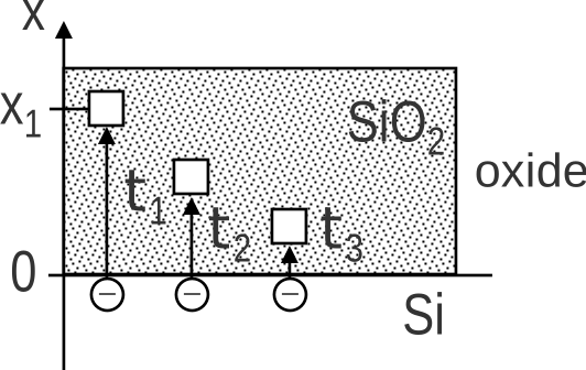
Consider a long-channel nMOS transistor which cross section is shown in Figure 21. The mobile carriers (electrons in the case of the n-channel transistor) which constitute the conductive channel may be trapped into traps located in the \(SiO_2\) or at the \(Si\)-\(SiO_2\) interface via tunneling effect. This process is characterized by a tunneling time constant \(\tau_t\) which depends exponentially on the distance \(x\) between the trap and the Si-\(SiO_2\) interface \[\begin{equation} \tau_t = \tau_0 \cdot e^{\alpha \cdot x}, \end{equation}\] where \(\alpha \cong 10^8\,cm^{-1}\). This trapping mechanism leads to a fluctuation of the number of carriers in the channel and therefore of the current. The PSD corresponding to the fluctuation \(\Delta N\) in number of electrons (holes) \(N\) due to a single trap having a tunneling time constant \(\tau_t\) is given by a Lorentzian PSD \[\begin{equation} S_{\Delta N}(f) = \overline{\Delta N^2} \cdot \frac{2 \tau_t}{1 + (2 \pi f \tau_t)^2}, \end{equation}\] where \(\overline{\Delta N^2}\) is the variance of \(\Delta N\). This variance \(\overline{\Delta N^2}\) can be assumed to be proportional to \(N\) and hence \(\overline{\Delta N^2} = \beta \cdot N\) resulting in \[\begin{equation} S_{\Delta N}(f) = \beta \cdot N \cdot \frac{2 \tau_t}{1 + (2 \pi f \tau_t)^2}. \end{equation}\] It can be shown that the PSD of the drain current fluctuations \(\Delta I_D\) resulting from the charge fluctuations in the channel due to a single trap is given by \[\begin{equation}\label{eqn:S_ID1} S_{\Delta I_D}(f) = \left(\frac{I_D}{N}\right)^2 \cdot S_{\Delta N}(f) \cong \frac{\beta \cdot I_D^2}{N} \cdot \frac{2 \tau_t}{1 + (2 \pi f \tau_t)^2}. \end{equation}\] \(\eqref{eqn:S_ID1}\) gives the PSD of the drain current fluctuation due to trapping of an electron in a single trap. To get the PSD of the drain current fluctuation due to all the traps located in the oxide, we need to average \(\eqref{eqn:S_ID1}\) over all the tunneling time constants comprised between \(\tau_{t,min}\) and \(\tau_{t,max}\). This results in a 1/f PSD within the frequency range comprised between \(1/(2 \pi \tau_{t,max})\) and \(1/(2 \pi \tau_{t,min})\) [15] \[\begin{equation} S_{\Delta I_D}(f) = \frac{1}{f} \cdot \frac{\beta \cdot I_D^2}{\pi N} \cdot \frac{\arctan(2 \pi f \tau_{t,max}) - \arctan(2 \pi f \tau_{t,min})}{\ln(\tau_{t,max}/\tau_{t,min})}. \end{equation}\]
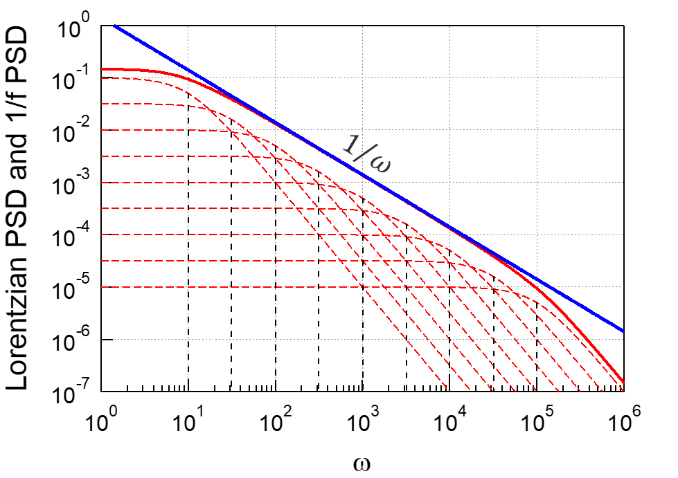
The above integration corresponds to summing all the Lorentzian curves corresponding to each trap resulting in a 1/f power spectrum. This is illustrated in the plot of Figure 22 with 9 Lorentzians equally spaced (in log scale) \[\begin{equation} S(\omega) = \frac{\tau_t}{1 + (\omega\,\tau_t)^2} = \cdot \frac{1/\omega_t}{1 + \left(\frac{\omega}{\omega_t}\right)^2}. \end{equation}\]
This same technique can be used in a circuit simulator to generate a 1/f noise PSD within a certain bandwidth from a white noise PSD.
3.3.3.2 The Hooge model
Another approach to explain the cause of 1/f noise is proposed by Hooge. In this model the current fluctuations are actually due to fluctuations of the mobility rather than the number of carriers in the channel. This is why it is called a volume effect rather than an interface effect like in the Mc-Worther model described above.
The PSD of the current fluctuations \(\Delta I\) in a semiconductor according to the Hooge model can be expressed as [16] [9] \[\begin{equation} S_{\Delta I}(f) = \frac{\alpha_H}{f \cdot N} \cdot I^2, \end{equation}\] where \(\alpha_H \cong 2 \times 10^{-3}\) is the unitless Hooge parameter that applies to a wide range of devices and materials [17].
Applied to the MOS transistor, the flicker noise is often referred to the gate (fluctuations of the gate voltage instead of fluctuations of the drain current). In strong inversion and saturation (with \(V_S=0\)), this model leads to a PSD [9] \[\begin{equation} S_{\Delta V_G}(f) \cong \frac{\alpha_H \cdot q \cdot (V_G-V_{T0})}{2 W \cdot L \cdot C_{ox} \cdot f} \end{equation}\] which is inversely proportional to the gate area \(W \cdot L\) and to \(C_{ox}\) and proportional to the overdrive voltage \(V_G - V_{T0}\).
3.3.4 Random telegraph noise (RTN)
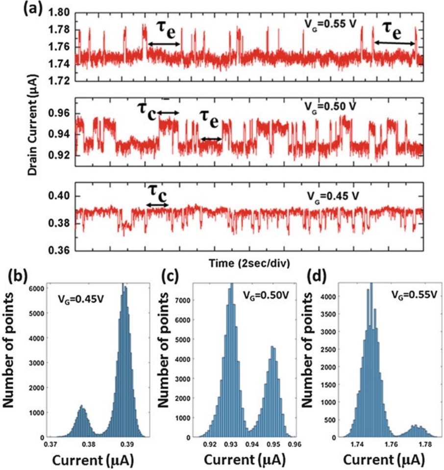
With the down-scaling of CMOS technologies as presented in Chapter 2, the area and drain current level of transistors have decreased significantly. This leads to abrupt variations of the drain current due to mobile charges in the channel being occasionally captured by a trap and then emitted back to the channel after a period time. This trapping mechanism is therefore changing the threshold voltage and hence the drain current according to [19] \[\begin{equation} \Delta V_T = \frac{q}{W \cdot L \cdot C_{ox}}, \end{equation}\] where \(W\) and \(L\) are the transistor gate width and length and \(C_{ox}\) is the oxide capacitance per unit area.
The dynamics at which the changes occur is characterized by the capture time constant \(\tau_c\) and the emission time constant \(\tau_e\). The left plot of Figure 23 shows the drain current versus time waveforms that have been measured on an nMOS transistor from a 22 nm FDSOI technology with \(W=80\,nm\) and \(L=100\,nm\) and which is affected by a single RTN trap [18]. The threshold voltage and hence the drain current is therefore switching between two values as illustrated in the top plots of Figure 24 [18]. We also see that the rate at which the current switches and the time it remains at a given level depend on the gate bias voltage. Indeed, looking at the top trace, corresponding to \(V_G = 0.55\,V\), the emission time constant is larger than the capture time constant (\(\tau_e > \tau_c\)) resulting in the current staying mostly at the lower level, roughly with a 6 to 1 ratio as shown by the corresponding histogram at the bottom of the figure. As the bias is lowered to \(V_G=0.5\,V\), the two time constants get closer to each other and the current stays on both levels with approximately a 1 to 2 ratio as shown in the middle plot. Finally, for \(V_G=0.45\,V\), the capture time constant is now larger than the emission time constant (\(\tau_e < \tau_c\)) and the current stays mostly on the top level.
The threshold voltage variations due to RTN can become a major challenge in down-scaled technologies. This is particularly the case for semiconductor memories like SRAM which noise margin is directly impacted [19] or in floating-gate non-volatile memories [20].
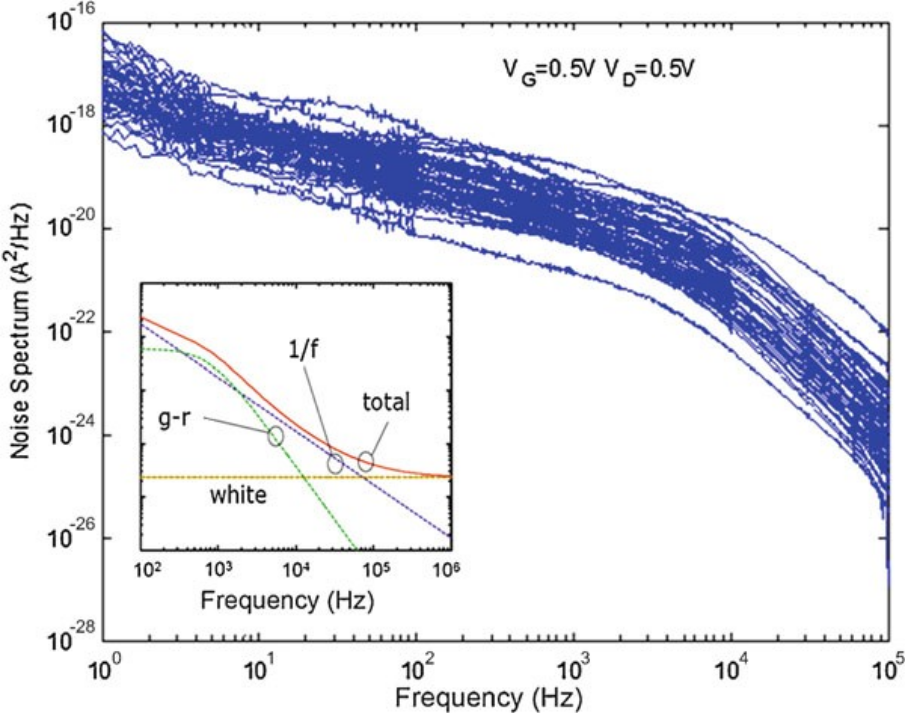
The PSD of the drain current fluctuation \(\Delta I_D\) normalized to the square of the drain current is given by \[\begin{equation} \frac{S_{\Delta I_D^2}(f)}{I_D^2} = \frac{\overline{\Delta N^2}}{N^2} \cdot \frac{4 \tau_r}{1 + (2\pi f \tau_r)^2}, \end{equation}\] where \[\begin{equation} \tau_r \triangleq \left(\frac{1}{\tau_c} + \frac{1}{\tau_e}\right)^{-1} \end{equation}\] is the carrier lifetime or effective time constant, \(\overline{\Delta N^2}\) is the variance of the fluctuation of the number of carriers \(N\) in the channel. Note that \(\overline{\Delta N^2}\) is proportional to the concentration of generation–recombination-trapping centers. It can be shown that the PSD of the current fluctuations due to a single trap is then a Lorentzian spectrum given by [18] \[\begin{equation} S_{\Delta I_D^2}(f) = 4 I_D^2 \cdot \frac{\tau_r}{\tau_c + \tau_e} \cdot \frac{4 \tau_r}{1 + (2\pi f \tau_r)^2}. \end{equation}\]
RTN does not appear alone, but is usually superimposed to the flicker and white noise, producing one or several bumps (depending on the number of active traps) in the 1/f part of the noise PSD as illustrated in Figure 24 [18].
3.3.5 Integrated white noise (Random Walk or Wiener Process)
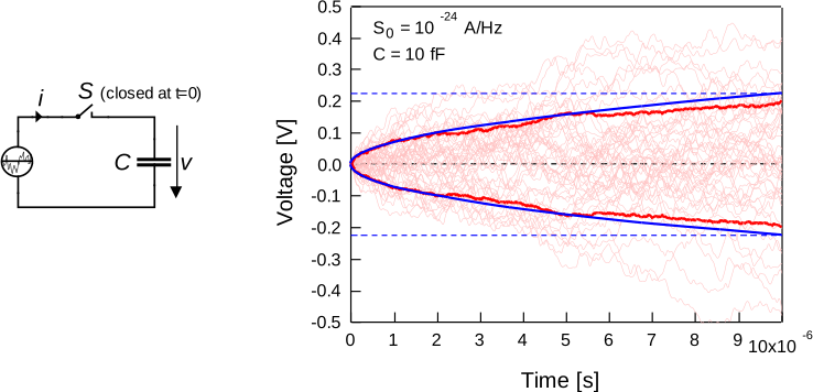
If a white noise current source with PSD and ACF given by \[\begin{equation} S_i(f) =S_0 \quad \text{and} \quad R_i(\tau) = S_0 \cdot \delta(\tau), \end{equation}\] is integrated on a capacitor \(C\) starting at time \(t=0\) as shown in Figure 25, it gives rise to a non-stationary (voltage) noise with an ACF given by \[\begin{align} R_{vv}(t,\tau) = \begin{cases} \frac{S_0}{C^2} \cdot t & \text{for $0 < t < T$}\\ \frac{S_0}{C^2} \cdot T & \text{for $0 < T < t$}. \end{cases} \end{align}\] The standard deviation of the voltage (rms value) is therefore increasing with \(\sqrt{t}\) as shown in Figure 25 which shows the results obtained from transient noise simulations.
We typically find this kind of noise at the output of a transimpedance amplifier (charge amplifier) connected to a photodiode generating shot noise.
3.4 Noise models of basic components
3.4.1 Resistor
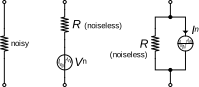
As shown in Figure 26, a noisy resistor can be modeled by a noiseless resistor in series with a noise voltage source having a zero average value and a (unilateral) PSD given by \[\begin{equation} S_{V_n} = 4 k_B\,T \cdot R \end{equation}\] where \(k_B = 1.38\times10^{-23}\,J/K\) is the Boltzmann constant and \(T\) the absolute temperature. It can also be modelled by a noiseless resistor in parallel with a noise current source having a zero mean value and a PSD given by \[\begin{equation} S_{I_n} = 4 k_B\,T \cdot G, \end{equation}\] where \(G=1/R\).
Which model to use depends very much on the circuit to be analyzed. When the signal is actually carried by a current (like for example inside an OTA), it is usually simpler to use the current source model, whereas when the signal is carried by a voltage it is better to use the voltage source.
Note that, contrary to shot noise, the noise PSD of thermal noise is independent of the current flowing through the resistor or the dc voltage across it, it only depends on the resistance \(R\) (conductance \(G=1/R\)) and on temperature \(T\).
3.4.2 Diode
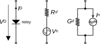
The noise of a diode is best modelled by adding a noise current source in parallel to a noiseless diode. Since the diode is a barrier controlled device it shows shot noise. The PSD of the noise current source is therefore given by \[\begin{equation} S_{I_n} = 2 q \cdot I_D. \end{equation}\] The noise PSD is proportional to the DC current flowing through the diode.
3.4.3 MOSFET
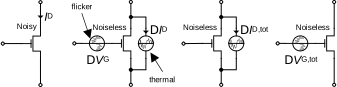
Figure 28 shows the noisy MOSFET in saturation which is modeled by a noiseless transistor to which two noise sources are added, namely a current noise source connected between the drain and the source and accounting for the thermal noise generated in the channel and a voltage noise source in series with the gate that models the flicker noise. The PSD of the thermal noise current source is given by \[\begin{equation} S_{\Delta I_D^2} = 4 k_B\,T \cdot G_{n} \end{equation}\] where \(G_n\) is the thermal noise conductance which is proportional to the gate transconductance \(G_m\) according to \[\begin{equation} G_n = \gamma_n \cdot G_m. \end{equation}\] Parameter \(\gamma_n\) is the thermal noise excess factor which for a long-channel transistor can be considered close to one. \(G_m\) is the gate transconductance which is bias dependent.
The PSD of the voltage source modeling the flicker noise is defined as \[\begin{equation} S_{\Delta V_G^2}(f) = \frac{K_F}{C_{ox}^{\alpha} \cdot W \cdot L \cdot f}, \end{equation}\] where \(K_F\) is a parameter that strongly depends on technology and is slightly bias-dependent, \(W\) and \(L\) are the transistor gate width and length, respectively. The exponent \(\alpha\) is typically equal to 2 for the Mc Worther model and 1 for the Hooge model. From a design perspective, the most important property is that the input-referred flicker noise is inversely proportional to the gate area \(W \cdot L\). The flicker noise can be expressed as if it would be thermal noise according to \[\begin{equation} S_{\Delta V_G^2}(f) = 4 k_B\,T \cdot R_n(f), \end{equation}\] where \(R_n(f)\) is the gate-referred noise resistance accounting for flicker noise and which is hence frequency-dependent \[\begin{equation} R_n(f) = \frac{\rho}{W \cdot L \cdot f} \end{equation}\] and \[\begin{equation} \rho = \frac{K_F}{4 k_B\,T\cdot C_{ox}^{\alpha}}. \end{equation}\]
We can calculate the total drain current fluctuations due to both thermal and flicker noise which is given by \[\begin{equation} S_{\Delta I_{D,tot}^2}(f) = S_{\Delta I_D^2} + G_m^2 \cdot S_{\Delta V_G^2}(f) = 4 k_B\,T \cdot G_{n,tot}(f) \end{equation}\] with \[\begin{equation} G_{n,tot}(f) = \gamma_n \cdot G_m + G_m^2 \cdot \frac{\rho}{W \cdot L \cdot f}. \end{equation}\]
In many cases it is more useful to refer the total noise to the gate as \[\begin{equation} S_{\Delta V_{G,tot}^2} =4 k_B\,T \cdot R_{n,tot}(f), \end{equation}\] with \[\begin{equation} R_{n,tot}(f) = \frac{\gamma_n}{G_m} + \frac{\rho}{W \cdot L \cdot f}. \end{equation}\]
The noise of the MOS transistor is discussed in much more details in Chapter~4, particularly how the above parameters relate to the bias point.
3.4.4 OPAMP
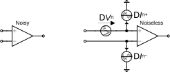
Moving to a higher level of abstraction, the noise of a complete OPAMP requires three noise sources: two current noise sources \(\Delta I_{n+}\) and \(\Delta I_{n-}\) and a noise voltage source \(\Delta V_n\) in series with the differential input voltage. Note that current noise sources can be ignored for high impedance OPAMP such CMOS OPAMPs.
3.5 Noise calculation in continuous-time circuits
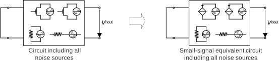
Since the noise fluctuations are usually small (i.e. \(\ll U_T=k_B\,T/q\) for voltage fluctuations), the circuit can be linearized around its operating point and the noise sources need to be added to the resulting linear circuit. For each of these noise sources, we first need to characterize its noise in terms of its PSD \(S_{n,k}(f)\). We then need to calculate all the transfer functions \(H_k(f)\) from the noise source to the output. Since the noise sources are coming from different devices they can be assumed to be uncorrelated. The PSD at the output is then given by \[\begin{equation} S_{nout}(f) = \sum_{k=1}^{K} |H_k(f)|^2 \cdot S_{n,k}(f). \end{equation}\]
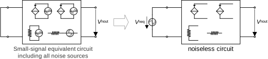
The noisy circuit can then modeled by a noiseless circuit with a single input-referred noise voltage source \(V_{neq}\) given by \[\begin{equation} S_{V_{neq}} = \frac{S_{nout}(f)}{|A_v(f)|^2}, \end{equation}\] and producing the same noise at the output as that of the noisy circuit having the input short-circuited, where \(A_v(f)\) is the voltage transfer function from the input to the output.