Common-source Stage Optimization using the Inversion Coefficient
In Closed-loop Configuration (Version 2)
Abstract
This notebook shows how to minimize the bias current of a common-source (CS) amplifier for achieving a given gain and bandwidth. Contrary to the open-loop case, the CS amplifier is in closed-loop (CL) configuration with a capacitive feedback.
1 Introduction
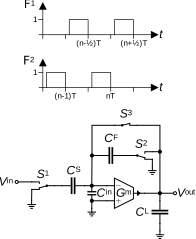
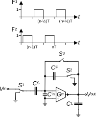
It is very common to find transconductors or operational transconductance amplifiers (OTAs) operating with a capacitive feedback. For example, we can find them in switched-capacitor (SC) amplifier as shown in Figure 1. This amplifier operates with two non-overlapping phases \(\Phi_1\) and \(\Phi_2\). During phase \(\Phi_1\), capacitor \(C_S\) is disconnected from the input and connected to ground. Similarly, the feedback capacitor \(C_F\) is disconnected from the output and connected to ground. If we assume that the OTA has a large DC gain, the negative input operates like a virtual ground so that both capacitors \(C_S\) and \(C_F\) are discharged. Switch S3 puts the OTA in voltage follower mode and keeps its output to ground (actually to its offset).
During phase \(\Phi_2\), \(C_S\) is connected back to the input, \(C_F\) back to the output and switch S3 is opened, putting the amplifier in amplification mode. Neglecting the OTA input capacitance \(C_{in}\), the ideal voltage gain is then given by \(-C_S/C_F\). So to have a large voltage gain \(C_F\) has to chosen small enough in order to maximize the gain but still larger than the parasitic capacitances.
Note
Note that the amplifier of Figure 1 is called an autozero (AZ) amplifier because it can cancel the OTA offset and reduce its low-frequency noise. To learn more about this topic please have a look at the Noise and offset reduction techniques Chapter of the book.
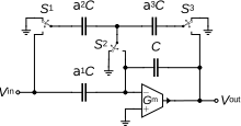
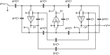
Another example of OTA with capacitive feedback can be found in SC filters as illustrated in Figure 2. Contrary to the amplifier case of Figure 1, in SC filters the sampling capacitances (like \(\alpha_1\,C\), \(\alpha_2\,C\) and \(\alpha_3\,C\) in Figure 2 (a)) are usually much smaller than the feedback capacitance. Their values can actually become close to the parasitic input capacitance \(C_{in}\) of the OTA.
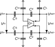
The SC amplifiers and filters are usually implemented as fully-differential circuits. The OTA with capacitance feedback in SC amplifiers and filters can then be drawn as shown in Figure 3 (a). If the voltages at the input and output are fully balanced, then the fully differential circuit of Figure 3 (a) can be reduced to the single-ended circuit shown in Figure 3 (b).
Note
Note that \(C_{in}\) represents the parasitic input capacitance of the OTA which corresponds to the gate-to-source capacitance of one transistor of the input differential pair.
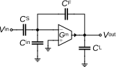
The simplest implementation of the circuit shown Figure 3 (b) is by replacing the OTA with a single transistor in common-source (CS) configuration as shown in Figure 4.
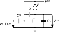
Similarly to what was done for the CS gain stage in open-loop configuration, we now want to check whether there is a minimum bias current to achieve a given gain-bandwidth product for the CS amplifier in closed-loop (CL) configuration shown in Figure 4.
2 Analysis
2.1 Small-signal Transfer Function
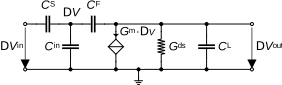
The small-signal schematic of the CL CS gain stage of Figure 4 is shown in Figure 5. Notice that we added the input capacitance \(C_{in}\) which essentially corresponds to the transistor gate-to-source and gate-to-bulk capacitances. The gate-to-drain capacitance is included in \(C_F\) and therefore needs to be de-embedded in the design. It is easy to show that the transfer function is given by \[\begin{equation} A(s) \triangleq \frac{\Delta V_{out}}{\Delta V_{in}} = A_0 \cdot \frac{1-s/\omega_z}{1+s/\omega_p} \end{equation}\] where \[\begin{align} A_0 &= A_{0,ideal} \cdot \frac{\beta \cdot A_{dc}}{1 + \beta \cdot A_{dc}} \cong A_{0,ideal}\quad\text{for $A_{dc} \gg 1$},\\ A_{0,ideal} &= -\frac{C_S}{C_F},\\ \omega_p &= \frac{1+\beta \cdot A_{dc}}{R_{ds} \cdot C_{out}} \cong \frac{\beta \cdot A_{dc}}{R_{ds} \cdot C_{out}} = \frac{\beta \cdot G_m}{C_{out}},\\ \omega_z &= \frac{G_m}{C_F}. \end{align}\]
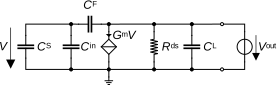
\(A_{dc} = G_m \cdot R_{ds}\) is the CS transistor DC voltage gain, \(\beta \cdot A_{dc}\) the DC loop gain where \(\beta\) is the feedback gain which can be calculated from the schematic shown Figure 6 as \[\begin{equation} \beta \triangleq \frac{V}{V_{out}} = \frac{C_F}{C_F + C_S + C_{in}}. \end{equation}\]
The amplifier bandwidth is given by \(\omega_c = \omega_p \cong \beta \cdot G_m/C_{out}\) where \(C_{out}\) is the total capacitance seen at the output and given by \[\begin{equation} C_{out} = C_L + (1-\beta) \cdot C_F = C_L + \frac{C_S + C_{in}}{C_F + C_S + C_{in}} \cdot C_F. \end{equation}\]
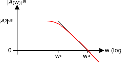
In order to achieve some DC gain, \(C_F\) is made smaller than \(C_S\) and usually also smaller than \(C_L\). This means that the right-hand side (RHS) zero is located higher than the unity gain frequency which is then simply given by \(\omega_u \cong G_m/C_{out}\). For frequencies below \(\omega_u\), the magnitude of the transfer function is shown in Figure 7.
2.2 Minimum current for a given bandwidth (long-channel)
When optimizing the CL CS amplifier for low current consumption, the transistor is often biased in moderate or even weak inversion leading to large transistor and therefore an increased input and output capacitance. If we assume that the transistor parasitic capacitance at the drain is much smaller than the load capacitance, we can neglect its impact on the output capacitance. On the other hand, twe input capacitance can be modeled as the sum of the gate-to-source and gate-to-bulk capacitances \[\begin{equation} C_{in} = C_{GS} + C_{GB}. \end{equation}\] Assuming that the transistor is biased in saturation, we have \[\begin{equation} C_{GS} \cong W\,L\,C_{ox} \cdot c_{gsi} + C_{GSo} \cdot W \end{equation}\] where \(c_{gsi}\) is the normalized intrinsic gate-to-source capacitance which is typically equal to \(2/3\) in strong inversion and is proportional to \(IC\) in weak inversion. \(C_{GSo}\) is the gate-to-source overlap capacitance per unit width.
The gate-to-bulk capacitance \(C_{GB}\) is given by \[\begin{equation} C_{GB} \cong \,W\,L\,C_{ox} \cdot c_{gbi} + C_{GBo} \cdot W, \end{equation}\] where \(c_{gbi}\) is the normalized gate-to-bulk intrinsic capacitance which in strong inversion is given by \[\begin{equation} c_{gbi} = \frac{n-1}{3n}. \end{equation}\] \(C_{GBo}\) is the gate-to-bulk overlap capacitance per unit width.
For a given transistor length \(L\), the input capacitance \(C_{in}\) scales with \(W\) according to \[\begin{equation} C_{in} = C_{GW} \cdot W, \end{equation}\] where \(C_{GW}\) is the gate-to-source and gate-to-bulk capacitance per unit width given by \[\begin{equation} C_{GW} = L\,C_{ox} \cdot (c_{gsi} + c_{gbi}) + C_{GSo} + C_{GBo}. \end{equation}\]
In order to achieve a certain bandwidth we need to have a certain transconductance for a certain load capacitance. In order to maximize the current efficiency, we should bias the transistor in weak inversion. This leads to a large transistor and therefore large parasitic capacitances which will impact the bandwidth. Imposing the bandwidth, at some point the capacitance becomes so large that it is no more possible to achieve the required transconductance in weak inversion for the desired bandwidth. Does this mean that there is a minimum current for the CL CS amplifier to achieve a certain bandwidth?
To answer this question we need to solve the following set of equations for \(I_b\) and \(W\) assuming a given length \(L\) \[\begin{align} \omega_c &= \beta \cdot \frac{G_m}{C_{out}},\\ C_{out} &= C_L + (1-\beta) \cdot C_F,\\ \beta &= \frac{C_F}{C_F + C_S + C_{in}},\\ C_{in} &= W \cdot C_{GW},\\ I_b &= I_{spec\Box} \cdot \frac{W}{L} \cdot IC,\\ G_m &= \frac{I_{spec\Box}}{n U_T} \cdot \frac{W}{L} \cdot g_{ms}(IC), \end{align}\] where \(g_{ms}(IC)\) is the long-channel normalized source transconductance given by \[\begin{equation} g_{ms} \triangleq \frac{G_{ms}}{G_{spec}} = \frac{G_{ms}\,U_T}{I_{spec}} = \frac{G_m\,n U_T}{I_{spec}}= \frac{\sqrt{4 IC + 1} - 1}{2} = \frac{2 IC}{\sqrt{4 IC + 1} + 1}. \end{equation}\] with \(I_{spec} = I_{spec\Box}\,W/L\).
Solving for \(I_b\) and \(W/L\) leads to the following normalized solutions \[\begin{align}\label{eq:ib_AR} i_b &\triangleq \frac{I_b}{I_{spec\Box} \cdot \Omega} = \frac{IC}{g_{ms}(IC) - \Theta},\\ AR &\triangleq \frac{W/L}{\Omega} =\frac{1}{g_{ms} - \Theta}, \end{align}\] where \[\begin{align} \Omega &\triangleq \frac{\omega_c}{\omega_L},\\ \omega_L &\triangleq \frac{I_{spec\Box}}{n U_T} \cdot \frac{1}{(1+C_S/C_L+C_S/C_F) \cdot C_L},\\ \Theta &\triangleq \frac{\omega_c}{\omega_W},\\ \omega_W &\triangleq \frac{I_{spec\Box}}{n U_T} \cdot \frac{1}{(1+C_L/C_F) \cdot C_{GW} \cdot L}. \end{align}\]
Note
Notice that we get the same equations for the normalized current \(i_b\) and normalized aspect ratio \(AR\) than what we obtained for the CS in open-loop configuration. Except that the normalization is now different.
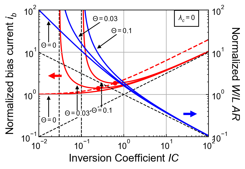
The normalized current \(i_b\) and aspect ratio \(AR\) are plotted versus the inversion coefficient \(IC\) in Figure 8 for different values of parameter \(\Theta\). The normalized current \(i_b\) is also plotted versus the inversion coefficient for more values of parameter \(\Theta\) in Figure 9.
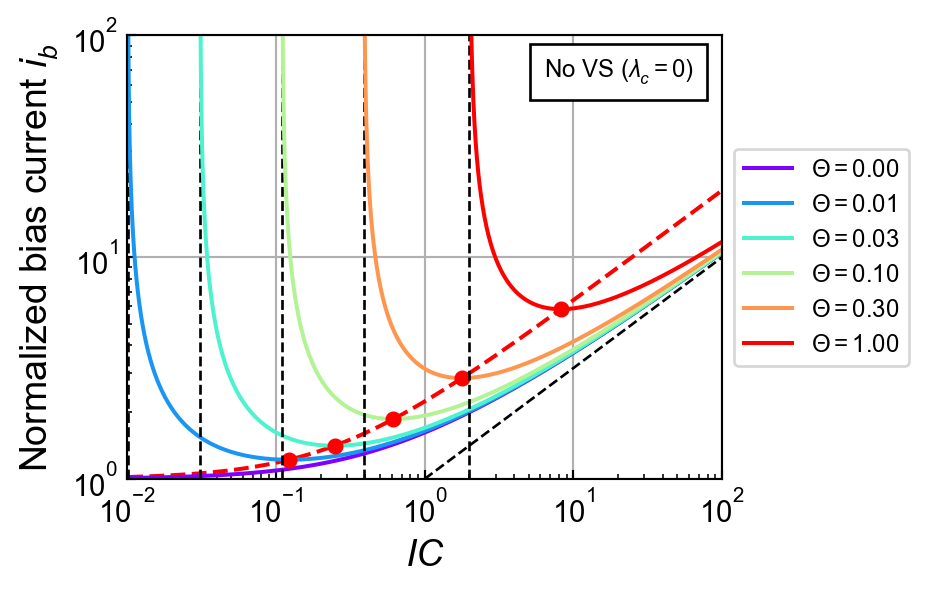
From Figure 8 and Figure 9, we clearly see that there is a minimum current for a given value of parameter \(\Theta\). We can find the optimum inversion coefficient \(IC_{opt}\) corresponding to this minimum current which is given by \[\begin{equation} \begin{split} IC_{opt} &= \left(\sqrt{\Theta \cdot (1+\Theta)} + \Theta + \frac{1}{2}\right)^2 - \frac{1}{4}\\ &= 2 \Theta \cdot (1+\Theta) + (1+2\Theta) \cdot \sqrt{\Theta \cdot (1+\Theta)}\\ &\cong 2 \Theta + \sqrt{\Theta} \;\; \textsf{for $\Theta \ll 1$}. \end{split} \end{equation}\]
We also see that there is a minimum inversion coefficient \(IC_{lim}\) below which the desired bandwidth \(\omega_c\) can no more be achieved \[\begin{equation} IC_{lim} = \Theta \cdot (1+\Theta) \cong \Theta, \end{equation}\] which is about equal to \(\Theta\) for small values of \(\Theta\).
The optimum normalized current is given by \[\begin{equation} i_{bopt} \triangleq i_b(IC_{opt}) = 1 + 2\Theta +2\sqrt{\Theta \cdot (1+\Theta)}. \end{equation}\]
The optimum current also corresponds to an optimum transistor width \(W\) and hence and optimum normalized \(W/L\) given by \[\begin{equation} AR_{opt} \triangleq AR(IC_{opt}) = \frac{1}{\sqrt{\Theta \cdot (1+\Theta)}}. \end{equation}\]
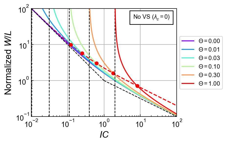
We see from Figure 10 that the transistor width increases first as \(1/\sqrt{IC}\) in strong inversion and then as \(1/IC\) in weak inversion making the transistor quickly very large until \(IC\) reaches \(IC_{lim}\) where the width becomes infinity. The dots correspond to the \(AR\) obtained for \(IC_{opt}\).
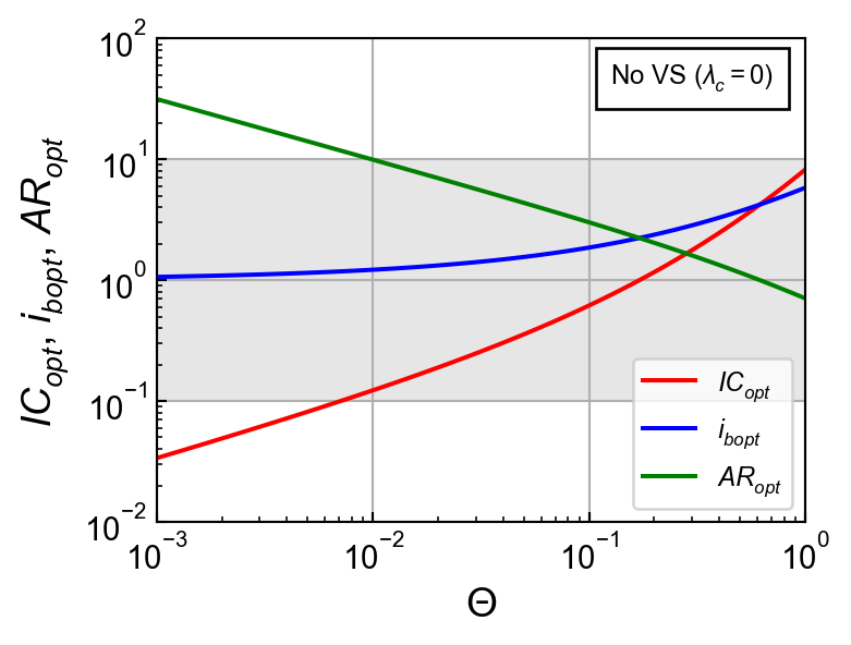
The optimum parameters \(IC_{opt}\), \(i_{bopt}\) and \(AR_{opt}\) are plotted versus \(\Theta\) in Figure 11. We can see that the optimum inversion coefficient is always located in moderate or eventually weak inversion.
We now will illustrate this optimization with a simple example.
3 Design Example
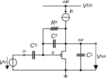
We want to size a CS SC amplifier of Figure 12 for the specifications given in Table 1. We need to find the minimum current and size the transistor to achieve this specs. Note that the feedback resistor \(R_F\) in Figure 12 has been added for biasing purpose and should be taken large enough not to limit the gain and bandwidth. The cut-off frequency due to \(R_F\) is given by \[\begin{equation} \omega_l = \frac{A_0}{R_F \cdot C_S} \end{equation}\] from which we deduce the value of \(R_F\) \[\begin{equation} R_F = \frac{A_0}{\omega_l \cdot C_S}. \end{equation}\] We will set \(f_l\) to 1 Hz.
| Specification | Symbol | Value | Unit |
|---|---|---|---|
| DC gain | \(A_0\) | 20 | \(dB\) |
| Bandwidth | \(BW\) | 100 | \(kHz\) |
| Load capacitance | \(C_L\) | 1 | \(pF\) |
| Feedback capacitance | \(C_F\) | 100 | \(fF\) |
| Transistor length | \(L\) | 1 | \(\mu m\) |
3.1 Process
We will design the CS CL amplifier for generic 180 nm bulk CMOS process. The physical parameters are given in Table 2, the global process parameters in Table 3 and finally the MOSFET parameters in Table 4.
| Parameter | Value | Unit |
|---|---|---|
| \(T\) | 300 | \(K\) |
| \(U_T\) | 25.875 | \(mV\) |
| Parameter | Value | Unit |
|---|---|---|
| \(V_{DD}\) | 1.8 | \(V\) |
| \(C_{ox}\) | 8.443 | \(\frac{fF}{\mu m^2}\) |
| \(W_{min}\) | 200 | \(nm\) |
| \(L_{min}\) | 180 | \(nm\) |
| Parameter | NMOS | PMOS | Unit |
|---|---|---|---|
| sEKV parameters | |||
| \(n\) | 1.27 | 1.31 | - |
| \(I_{{spec\Box}}\) | 715 | 173 | \(nA\) |
| \(V_{{T0}}\) | 0.455 | 0.445 | \(V\) |
| \(L_{{sat}}\) | 26 | 36 | \(nm\) |
| \(\lambda\) | 20 | 20 | \(\frac{{V}}{{\mu m}}\) |
| Overlap capacitances parameters | |||
| \(C_{{GDo}}\) | 0.366 | 0.329 | \(\frac{{fF}}{{\mu m}}\) |
| \(C_{{GSo}}\) | 0.366 | 0.329 | \(\frac{{fF}}{{\mu m}}\) |
| \(C_{{GBo}}\) | 0 | 0 | \(\frac{{fF}}{{\mu m}}\) |
| Junction capacitances parameters | |||
| \(C_J\) | 1 | 1.121 | \(\frac{{fF}}{{\mu m^2}}\) |
| \(C_{{JSW}}\) | 0.2 | 0.248 | \(\frac{{fF}}{{\mu m}}\) |
| Flicker noise parameters | |||
| \(K_F\) | 8.1e-24 | 6.8e-23 | \(J\) |
| \(AF\) | 1 | 1 | - |
| \(\rho\) | 0.05794 | 0.4828 | \(\frac{{V \cdot m^2}}{{A \cdot s}}\) |
| Matching parameters | |||
| \(A_{{VT}}\) | 5 | 5 | \(mV \cdot \mu m\) |
| \(A_{{\beta}}\) | 1 | 1 | \(\% \cdot \mu m\) |
| Source and drain sheet resistance parameter | |||
| \(R_{{sh}}\) | 600 | 2386 | \(\frac{{\Omega}}{{\mu m}}\) |
| Width and length parameters | |||
| \(\Delta W\) | 39 | 54 | \(\,nm\) |
| \(\Delta L\) | -76 | -72 | \(\,nm\) |
Note
Since in this example we end up with a large and long transistor, we can neglect the width and length reduction \(\Delta W\) and \(\Delta L\) and consider that \(W \cong W_{eff}\) and \(L \cong L_{eff}\).
We first need to estimate the parameter \(C_{GW}\) which is related to the transistor input capacitance \(C_{in}\). Since we don’t know the inversion coefficient we cannot estimate \(c_{gsi}\) and \(c_{gbi}\). We therefore will take their values in strong inversion for the estimation of the input capacitance per width \(C_{GW}\) \[\begin{equation} C_{GW} \cong \left(1-\frac{1}{3 n}\right) \cdot C_{ox} \cdot L + C_{GSo} + C_{GBo}, \end{equation}\] which depends on transistor length \(L\). Since the above theory was developed for a long-channel device, we will choose \(L =\) 1 \(\mu m\). We can now estimate the total gate capacitance per unit width for an n-channel transistor.
For the selected technology, we get \(C_{GW} =\) 6.596 \(fF/\mu m\).
From the DC gain specification \(A_0 =\) 10, we get \(C_S =\) 1 \(pF\). We can compute the optimum inversion coefficient \(IC_{opt}\), optimum width \(W_{opt}\), optimum current \(I_{b,opt}\) and aspect ratio \(\left.W/L\right|_{opt}\) which are given in Table 5.
| Parameter | Value | Unit |
|---|---|---|
| \(A_0\) | 10 | - |
| \(C_S\) | 1 | \(pF\) |
| \(f_L\) | 288.269 | \(kHz\) |
| \(f_W\) | 47.679 | \(MHz\) |
| \(\Omega\) | 0.347 | - |
| \(\theta\) | 0.002097 | - |
| \(IC_{opt}\) | 0.05 | - |
| \(i_{b,opt}\) | 1.096 | - |
| \(AR_{opt}\) | 21.813 | - |
| \(\left(\frac{W}{L}\right)_{opt}\) | 7.567 | - |
| \(I_{b,opt}\) | 272 | \(nA\) |
| \(W_{opt}\) | 7.57 | \(\mu m\) |
| \(C_{in}\) | 49.908 | \(fF\) |
| \(C_{GD}\) | 2.773 | \(fF\) |
| \(C_F\) | 100 | \(fF\) |
| \(C_{F0}\) | 97.227 | \(fF\) |
| \(R_F\) | 0.159 | \(T \Omega\) |
| Transistor | \(W\;[\mu m]\) | \(L\;[\mu m]\) | \(I_D\;[nA]\) | \(I_{{spec}}\;[nA]\) | \(IC\) | \(V_G-V_{{T0}}\;[mV]\) | \(V_{{DSsat}}\;[mV]\) |
|---|---|---|---|---|---|---|---|
| M1 | 7.57 | 1.00 | 272 | 5410 | 0.050 | -60 | 104 |
| Transistor | \(G_{{spec}}\;[\mu A/V]\) | \(G_{{ms}}\;[\mu A/V]\) | \(G_m\;[\mu A/V]\) | \(G_{{ds}}\;[nA/V]\) | \(\gamma_n\) |
|---|---|---|---|---|---|
| M1 | 209.093 | 10.024 | 7.885 | 13.591 | 0.645 |
The transistor size and bias information are given in Table 6, while Table 7 gives the small-signal parameters.
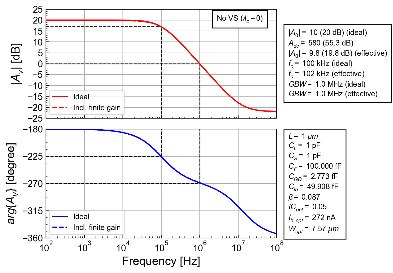
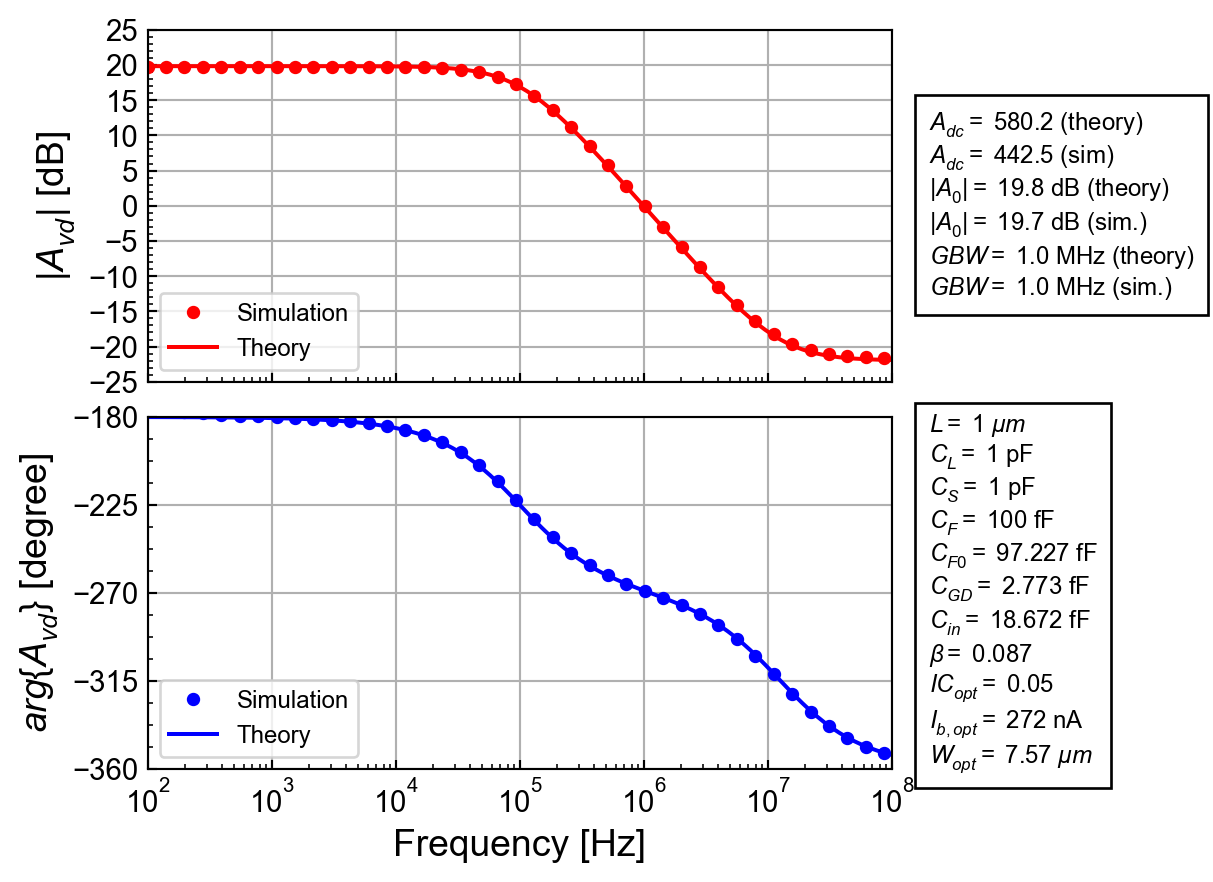
Having all the parameters, we can now calculate the theoretical transfer function which is plotted in Figure 13. We see that the DC gain and bandwidth are achieved.
3.2 Simulation results from ngspice
The theoretical results can be validated by comparing them to the results obtained from simulations performed with ngspice. In order to run the simulations you need to have ngspice installed. Please refer to the ngspice instructions.
Note
The simulations are performed with ngspice [1] using the EKV 2.6 compact model [2]. For ngspice, we use the original Verilog-A implementation of EKV 2.6 [3] modified by C. Enz to get the operating point informations and available on the Gitub va-models site provided by D. Warning at [4]. The parameters correspond to a generic 180 nm bulk CMOS process [5].
Before running the AC simulation, we first need to check the quiescent voltages and currents and the operating point by running an .OP simulation. The node voltages are extracted from the .ic file and presented in Table 8.
| Node | Voltage |
|---|---|
| vdd | 1.8 |
| in | 0 |
| g | 0.382048 |
| out | 0.382048 |
| Transistor | \(I_D\;[nA]\) | \(I_{spec}\;[nA]\) | \(IC\) | \(n\) | \(V_{Dsat}\;[mV]\) |
|---|---|---|---|---|---|
| M1 | 274 | 6034 | 0.045 | 1.27 | 114 |
| Transistor | \(n\) | \(G_{ms}\;[\mu A/V]\) | \(G_m\;[\mu A/V]\) | \(G_{mb}\;[\mu A/V]\) | \(G_{ds}\;[nA/V]\) |
|---|---|---|---|---|---|
| M1 | 1.27 | 10.145 | 7.835 | 2.292 | 17.705 |
The large-signal transistor bias information and the small-signal parameters extracted from the simulation are given in Table 9 and Table 10, respectively. We see that their values are very close to the theoretical values given in Table 6 and Table 7.
The simulated transfer function is shown in Figure 14 and compared to the theoretical transfer function of Figure 7. We see a perfect match between theory and simulation. Contrary to the open-loop analysis, in this example we don’t need to account for the transcapacitance \(C_m\) simply because its is much smaller than the chosen feedback capacitance \(C_F\).
Question
Is this truly the minimum current?
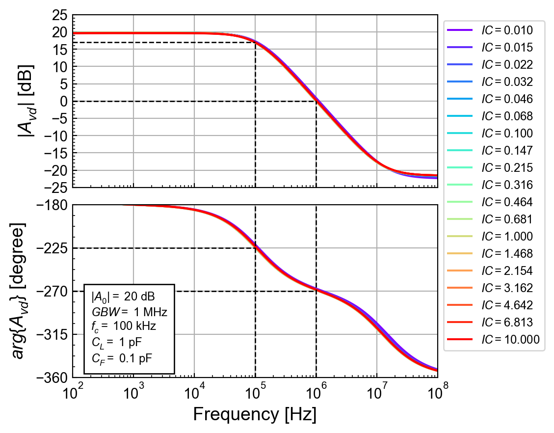
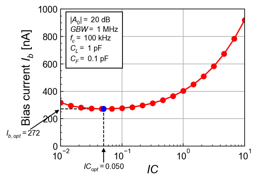
We can check this by sweeping \(IC\) and running a simulation for each of these point keeping the same specifications as in Table 1. This leads to the family of transfer functions shown in Figure 15. We see that all the simulations match the specification for different bias currents. The actual bias currents are plotted versus the inversion coefficient in Figure 16. We see that the bias current is indeed minimum at the theoretical value extracted above.
Note
We observe that the minimum is rather flat and therefore not too sensitive to the value of the optimum inversion coefficient.
4 Conclusion
In this notebook we have optimized a single transistor SC amplifier for minimum power consumption. We started to analyze the circuit accounting for the input parasitic capacitance which scales with the width of the transistor. We have found that there is an optimum transistor inversion coefficient and width for achieving a certain bandwidth with a minimum bias current. We then illustrated the theory with an example designed for a generic 180 nm bulk CMOS process. The sized circuit was then simulated with ngspice using the EKV 2.6 compact model. The simulation results perfectly match the theory.
This optimization process can be appplied to any differential OTA with capacitive feedback as can be found in SC amplifiers and filters. This is because the transconductance of the OTA is set by the input differential pair and the parasitic input capacitance is therefore equal to the parasitic capacitances of each transistor of this differential pair.
5 References
[1]
Holger Vogt, Giles Atkinson, Paolo Nenzi, “Ngspice User’s Manual Version 43.” https://ngspice.sourceforge.io/docs/ngspice-43-manual.pdf, 2024.
[2]
M. Bucher, C. Lallement, C. Enz, F. Théodoloz, and F. Krummenacher, “The EPFL-EKV MOSFET Model Equations for Simulation.” https://github.com/chrisenz/EKV/blob/main/EKV2.6/docs/ekv_v26_rev2.pdf, 1998.
[3]
W. Grabinski et al., “FOSS EKV2.6 verilog-a compact MOSFET model,” in European solid-state device research conference (ESSDERC), 2019, pp. 190–193. doi: 10.1109/ESSDERC.2019.8901822.
[4]
Dietmar Warning, “Verilog-A Models for Circuit Simulation.” https://github.com/dwarning/VA-Models, 2024.
[5]
W. Grabinski et al., “FOSS EKV 2.6 parameter extractor,” in 2015 22nd international conference mixed design of integrated circuits & systems (MIXDES), 2015, pp. 181–186. doi: 10.1109/MIXDES.2015.7208507.