| Variable | Normalization factor |
|---|---|
| Voltages | \(U_T \triangleq \frac{{k_B\,T}}{{q}}\) |
| with \(k_B\) the Boltzmann constant, | |
| \(T\) the absolute temperature and | |
| \(q\) the elementary charge | |
| Currents | \(I_{{spec}} = I_{{spec\Box}} \cdot \frac{{W}}{{L}} = 2n\,\beta\,U_T^2\) |
| with \(I_{{spec\Box}} \triangleq 2n\,\mu\,C_{{ox}}\,U_T^2\) and | |
| \(\beta \triangleq \mu C_{{ox}}\,\frac{{W}}{{L}} = \frac{{I_{{spec}}}}{{2n\,U_T^2}}\) | |
| Conductances | \(G_{{spec}} \triangleq \frac{{I_{{spec}}}}{{U_T}} = 2n\,\mu\,C_{{ox}}\,\frac{{W}}{{L}}\,U_T\) |
| Charge densities | \(Q_{{spec}} \triangleq -2n\,C_{{ox}}\,U_T\) |
| with \(C_{{ox}}\) the oxide capacitance per unit area and | |
| \(n\) the slope factor | |
| Distance \(x\) | \(\xi \triangleq \frac{{x}}{{L}}\) |
Analog Integrated Circuits Design using the Inversion Coefficient
Preview Edition
Licensing
This document is licensed under the Creative Commons License CC BY-NC-SA 
4 The Long-channel MOSFET Model
4.1 Introduction
With the stringent requirements on energy consumption of electronic devices, the Internet of Things (IoT) has become the primary driver for the design of low-power analog and RF circuits [1]. The implementation of increasingly complex functions under highly constrained power and area budgets, while circumventing the challenges posed by modern device technologies, makes the analog/RF design exercise ever more challenging. The designer often needs to make optimum choices to achieve the required gain, current efficiency, bandwidth, linearity and noise performance [2], [3]. To this purpose, he often starts his new design using simple transistor models to explore the design space and identify the region offering the best trade-off, before fine tuning his design by running more accurate simulations using the full fetched compact model available in the design kit [4], [5]. This task has been made more difficult in advanced CMOS technologies due to the down-scaling of CMOS processes and the reduction of the supply voltage, which has progressively pushed the operating point from the traditional strong inversion (SI) region towards moderate (MI) and even weak inversion (WI), where the simple quadratic model is obviously no more valid [6], [7], [8], [9]. This has led to an increasing interest in the EKV MOSFET model and the concept of inversion coefficient as the main design parameter replacing the overdrive voltage even for advanced technologies [10], [11].
4.1.1 Compact Models
The models of the MOS transistor that are available in circuit simulators like Spectre and ELDO are called compact models (CMs). El-Mansy and Boothroyd proposed the following definition of compact models [12], [13]:
compact models need to characterize the device accurately over a wide range of operating conditions, in a manner acceptable to the circuit designer, and with the capability of efficient computer implementation of the model. In order to achieve these objectives, he commonly employs a combination of device physics, approximation techniques, and insight in regard to the route to his goal which is likely to be the most successful. In the interests of the best representation of first-order physical behavior of the device in the working context, he is prepared to sacrifice accuracy of representation of what he judges to be second-order effects*. CMs usually correspond to a set of equations which describe the operation of the device in various mode of operation. They are customized for a given technology by a set of parameters that is called parameter deck which is part of the physical design kit (PDK) provided by foundries. In this sense CMs also represent the link between the technology and the circuit designers.
In the early days, CMs only needed less than ten parameters. With the developments of advanced technologies these CMs have now become more and more complex requiring many parameters (a few hundred parameters). These models are used in circuit simulators for verification to check whether the circuit achieves the required specifications, but they have become too complex to be easily used for the early pre-simulation phase. This is why it is useful to have a simpler model that captures the main features of the technology and guides the designer for choosing the right operating point for each transistor. The latter operating point is defined by the dc bias current and the width and length of each transistor.
4.1.2 Design Trade-offs
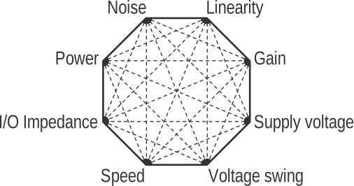
The design of analog circuits is the art of finding the right trade-off between conflicting constraints or specifications such as power, noise, linearity, gain, supply voltage, voltage swing, speed and input/output impedance as illustrated by Razavi’s analog design octahedron shown in Figure 1 [14]. Analog circuit design is therefore a complex exercise involving multiple tradeoffs. The design of analog and RF circuits in advanced nano-scale CMOS technologies sets special requirements on the CM (accuracy over a wide range of bias and geometries, speed, scalability, etc). Design in nano-scale CMOS technology nodes is further complicated because of the dominant short-channel effects (SCE). Modern circuit simulators coupled with sophisticated CM are powerful tools for the design and analysis of circuits in advanced technology nodes, yet most experienced analog designers would still rely on their design intuition and do ``hand calculations’’ before performing any simulation. This pre-simulation phase requires a stripped-down version of the model which is simple enough for initial design guidance, yet accurate enough to minimize trial-and-error simulation attempts.
The EKV model, with only 4 parameters (for bulk), can be used for this pre-simulation phase. The long-channel EKV model is presented below, starting with the static (DC) model.
4.1.3 Moderate and weak inversion in advanced CMOS technologies
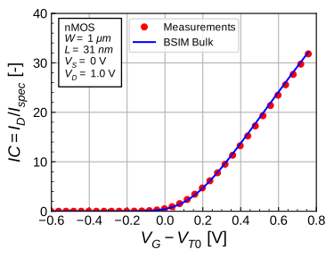
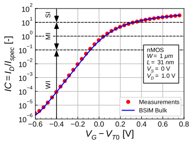
Figure 2 (a) shows the drain current \(I_D\) normalized to the specific current \(I_{spec}\) (which will be defined later) which corresponds to the inversion coefficient \(IC\) versus the overdrive voltage \(V_G-V_{T0}\) of a minimum length n-channel transistor from a 28-nm bulk CMOS technology [6], [7], [8], [9]. The first thing we observe is that the \(I_D\)-\(V_G\) characteristic is linear instead of being quadratic which is due to the effect of velocity saturation occurring for short-channel devices. Velocity saturation will be discussed in details in the Short-channel Chapter. We also note that strong inversion (SI) covers a wide range of voltage (roughly from 0.3 V to 0.8 V), however it actually only spans over a very small range of current. This can be better observed in Figure 2 (b) which is the same data than in Figure 2 (a) but with a logarithmic y-axis. The different regions of operation are identified as follows: strong inversion (SI) occurs for an inversion coefficient \(10 < IC\), moderate inversion (MI) correspond to \(0.1 < IC < 10\), whereas weak inversion (WI) occurs for \(IC < 0.1\). We now discover that MI and WI span over 6 decades of current, whereas SI is limited to less than 1 decade [6], [7], [8], [9]!
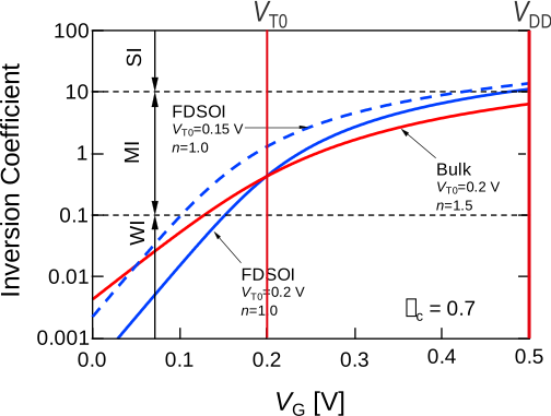
Additionally, because of the voltage scaling resulting from the down-scaling of CMOS technologies, the SI part is shrinking and will progressively disappear at low-voltage in advanced CMOS technologies for the benefit of MI and WI. This is illustrated in Figure 3 for various CMOS technologies. We have seen that the supply voltage will progressively reach 0.5 V in advanced technologies. If for example we look at a bulk nMOS transistor with a threshold voltage as low as 0.2 V and a slope factor \(n = 1.5\), assuming that the supply voltage is set at 0.5 V, as shown in Figure 3, the transistor does not even reach SI! Things improve slightly for a fully depleted SOI (FDSOI) technology. For a long channel transistor, in FDSOI the slope factor is close to 1. Assuming an nMOS transistor with the same threshold voltage but an ideal slope factor \(n=1\), we see that the transistor just reaches SI at \(V_{DD} = 0.5\,V\). FDSOI has this unique property that the threshold voltage can be adjusted with the back-gate voltage. Assuming it can be reduced from 0.2 V to 0.15 V, we observe that the device now just barely enters in SI at \(V_G = V_{DD}\). We can conclude that SI is progressively disappearing at low-voltage for advanced technologies.
The reduction of the supply voltage is therefore pushing the transistor operating point from the traditional SI region, towards MI and eventually SI. Additionally, we will show later that the optimum bias point often happens to be in MI. It is therefore essential to have a simple model that covers all regions of inversion and particularly MI and WI. How to derive a simple model that is valid in all regions of operations? We will show below how the EKV model can address this issue.
4.2 The static model
4.2.1 Device structure
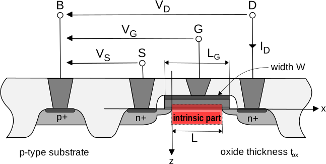
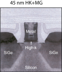
Figure 4 (a) shows the cross-section of a n-channel bulk MOS transistor taken from source to drain. We see that the structure is symmetrical with respect to source and drain. To take advantage of this symmetry and assuming that the doping is uniform from source to drain, at least in the channel region just below the oxide capacitance, we can refer the terminal voltages to the local substrate. The latter can either be the substrate or the well depending on the technology and the type of device. This means that the gate, source and drain voltages \(V_G\), \(V_S\) and \(V_D\) correspond actually to \(V_{GB}\), \(V_{SB}\) and \(V_{DB}\). As we will see later, this choice will lead to a symmetrical electrical model with respect to source and drain [15]. This symmetry is illustrated in Figure 4 (b) which represents a photo of the cross-section from a 45 nm bulk CMOS technology. Even if the dimensions are not at scale, we clearly see that the real device is indeed symmetrical with respect to source and drain.
In this section, we will focus mostly on the so-called intrinsic channel region delimited by the source and drain diffusions and the oxide capacitance highlighted by the red rectangle shown in Figure 4 (a). Indeed, even if this region is rather small compared to the actual extrinsic region, as shown by the cross-section of a real transistor shown in Figure 4 (b), it still represents the active part of the device which provides the transconductance and the intrinsic voltage gain required by analog circuits.
The transistor length \(L\) is defined by the channel length between the source and drain junctions which is different from the drawn gate length \(L_G\). The transistor width is \(W\) and the oxide thickness \(t_{ox}\). For a n-channel transistor, the drain current is defined positive entering the drain terminal.
Important
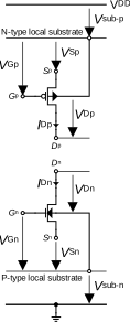
All the equations that will be derived below for the n-channel transistor remain valid for a p-channel transistor if the sign of the current and voltages are changed (i.e. \(I_{DS} \rightarrow I_{SD}\), \(V_{GB} \rightarrow V_{BG}\), \(V_{SB} \rightarrow V_{BS}\) and \(V_{DB} \rightarrow V_{BD}\)). The voltages and currents convention is summarized in Figure 5.
4.2.2 Drain current expression
The drain current \(I_D\) is given by the following differential equation [15] \[\begin{equation}\label{eqn:4:id_di_dv_dx} I_D = \mu \cdot W \cdot (-Q_i) \cdot \frac{dV}{dx}, \end{equation}\]
Note
It can be shown that \(\eqref{eqn:4:id_di_dv_dx}\) includes both the drift and the diffusion current components by making use of the channel voltage \(V\) which is equal to the quasi-Fermi potential of electrons in the channel [16].
where:
- \(\mu\) is the electron mobility in the channel region which will be considered as constant along the channel.
- \(V\) is the channel voltage defined as the quasi-Fermi voltage of electrons which is equal to the source voltage \(V_S\) at the source end of the channel (\(x=0\)) and to the drain voltage \(V_D\) at the drain end of the channel (\(x=L\)).
- \(Q_i\) is the inversion charge density corresponding to the mobile charge per unit area (electrons in the case of this n-channel transistor) and participating to the drain current.
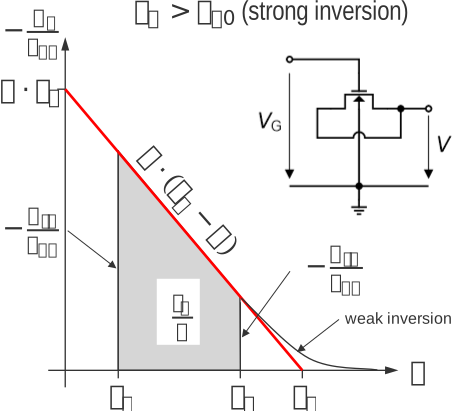
This inversion charge \(Q_i\) is obviously a function of the terminal voltages. If we bias the gate voltage \(V_G\) at a voltage larger than the threshold voltage \(V_{T0}\) (which will be defined below), minority carriers (electrons) are attracted towards the surface and form a channel below the oxide. If additionally we connect the source and drain voltage together as shown in the schematic of Figure 6 and connect it to a voltage \(V\), then this channel is uniform from source to drain, meaning that \(-Q_i\) is constant along the channel from source to drain. It can be shown that if we sweep the channel voltage \(V\) keeping the gate voltage \(V_G\) constant, the inversion charge \(-Q_i\) decreases with respect to the channel voltage \(V\) according to [15] \[\begin{equation}\label{eqn:4:qi_si} -\frac{Q_i}{C_{ox}} \cong n \cdot(V_P-V), \end{equation}\] until it reaches zero at the particular value of the channel voltage called the pinch-off voltage \(V_P\). When increasing the gate voltage, the inversion charge increases and the curve in Figure 6 moves upwards. The pinch-off intersection point then moves to the right and the pinch-off voltage increases with the gate voltage. Hence, the pinch-off voltage depends on the gate voltage and can be approximated by [15] \[\begin{equation}\label{eqn:4:vp_approx} \boxed{ V_P \cong \frac{V_G-V_{T0}}{n}, } \end{equation}\] where \(V_{T0}\) is the threshold voltage and \(n\) the slope factor which also corresponds to the slope of the linear approximation of \(-Q_i/C_{ox}\) shown in Figure 6 [15].
Note
Note that the slope factor \(n\) slightly decreases with the gate voltage from typically 1.6 in weak inversion to about 1.2 in strong inversion [15]. In the EKV model we ignore this dependence and consider \(n\) as constant with a value between 1.2 and 1.6. Usually taking \(n=1.3\) for a long-channel bulk transistor is a good trade-off.
The actual drain current is obtained by integrating \(\eqref{eqn:4:id_di_dv_dx}\) with respect to the channel voltage from the source, where \(V=V_S\), to the drain, where \(V=V_D\), resulting in [15] \[\begin{equation}\label{eqn:4:id} I_D = \beta \cdot \int_{V_S}^{V_D} \frac{-Q_i}{C_{ox}} \cdot dV = \frac{n\cdot\beta}{2} \cdot \left[(V_P-V_D)^2\ - (V_P-V_S)^2\right], \end{equation}\] where \(\beta \triangleq \mu \cdot C_{ox} W/L\) is the transconductance factor. As shown in Figure 6, the drain current corresponds to the area below the \(Q_i\) curve delimited by the source and drain voltages. If we increase the drain voltage keeping the source voltage constant, the drain current then increases until the drain voltage reaches the pinch-off voltage. The drain current then saturates to a constant value even if the drain voltage increases beyond the pinch-off voltage. As we will see later this mode of operation (e.g. \(V_P < V_D\)) is called forward saturation, whereas the linear region is defined for \(V_D < V_P\).
4.2.3 Forward and reverse currents
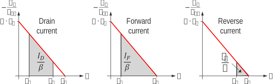
Taking advantage of the symmetry of the device, we can decompose the drain current into the difference between a forward component \(I_F\) minus a reverse component \(I_R\). As shown in Figure 7, this corresponds to split the drain current into the difference between the area of the large triangle corresponding to \(I_F\) as shown in the middle figure of Figure 7, and the area of the smaller triangle corresponding to \(I_R\) as shown in the right figure of Figure 7.
In a more formal way, it simply corresponds to split the integral in \(\eqref{eqn:4:id}\) into [15] \[\begin{equation}\label{eqn:4:IF_IR_def} I_D = \underbrace{\beta \cdot \int_{V_S}^{V_P} \frac{-Q_i}{C_{ox}} \cdot dV}_{\text{forward current }I_F} - \underbrace{\beta \cdot \int_{V_D}^{V_P} \frac{-Q_i}{C_{ox}} \cdot dV}_{\text{reverse current }I_R} = I_F - I_R \end{equation}\] with \[\begin{align} I_F &\triangleq \mathcal{F}(V_P-V_S),\\ I_R &\triangleq \mathcal{F}(V_P-V_D), \end{align}\] where \(\mathcal{F}\) is the same function giving the forward current as a function of \(V_P-V_S\) and the reverse current as a function of \(V_P-V_D\) according to [15] \[\begin{equation}\label{eqn:4:F} \mathcal{F}(V_x) \triangleq \beta \cdot \int_{V_x}^{V_P} \frac{-Q_i}{C_{ox}} \cdot dV. \end{equation}\]
Note that the above derivation was done assuming the transistor is biased in strong inversion (\(V_G > V_{T0}\)) ignoring moderate and weak inversion. In reality the inversion charge \(-Q_i\) never crosses zero as shown in Figure 6, but starts to decay exponentially to tend asymptotically to zero for large values of the channel voltage \(V\). Although the decomposition of the drain current into a forward and reverse current was defined in Figure 7 for a transistor biased in strong inversion, it also holds in all modes of inversion from weak to moderate and strong inversion by replacing the upper bound of the integral in \(\eqref{eqn:4:F}\) \(V_P\) by \(+\infty\) [15].
Note also that this decomposition of the drain current is only valid for long-channel transistors. Indeed, for short-channel devices, the effect of velocity saturation introduces a dependence of the velocity and hence of the mobility to the longitudinal direction \(x\) and this decomposition does not hold anymore [15].
4.2.4 Modes of operation (in voltage domain)
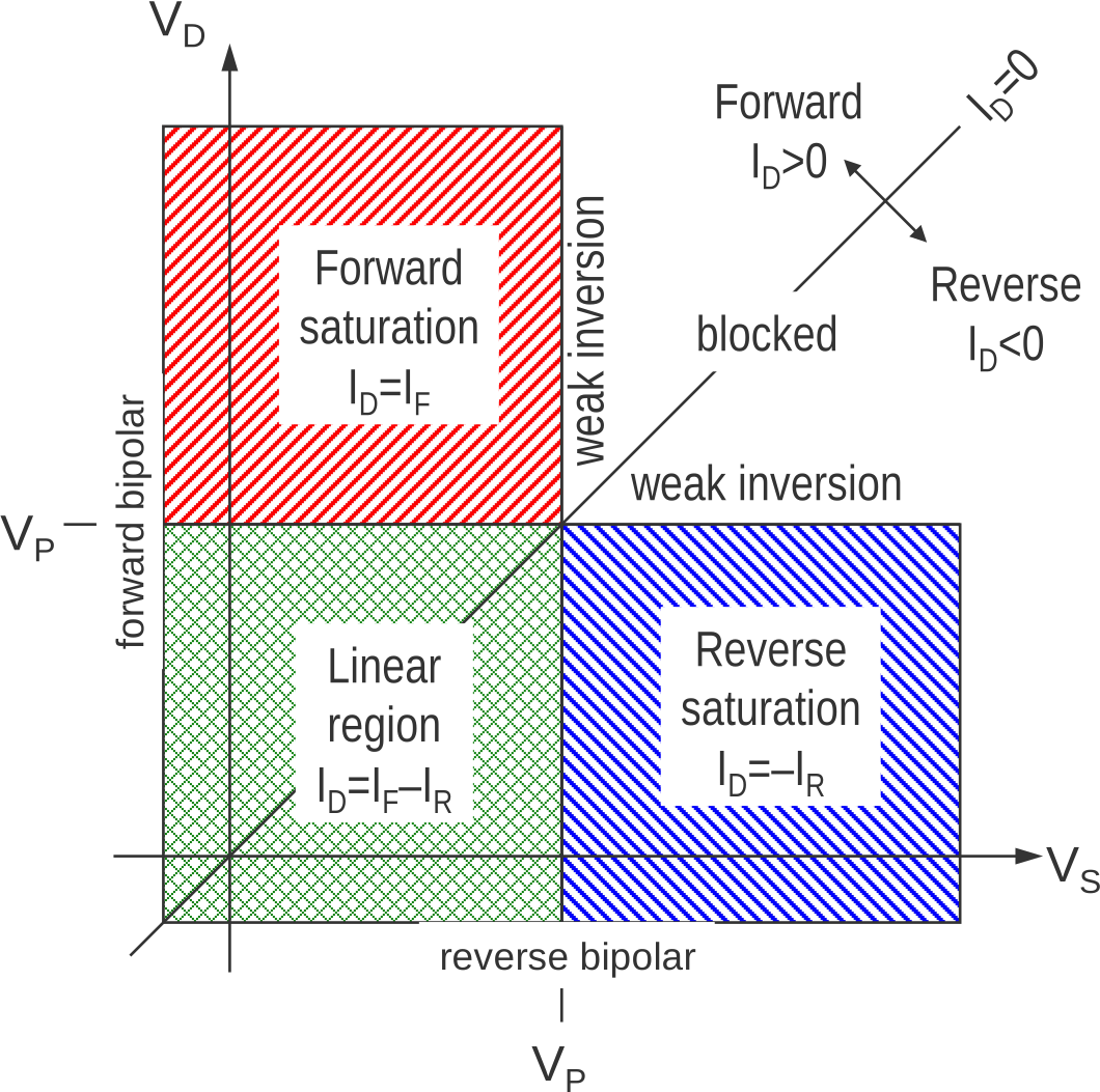
For a given gate voltage larger than the threshold voltage (transistor in strong inversion), the pinch-off voltage is larger than zero and splits the \(V_D\)-\(V_S\) plan into four different operation regions. When \(V_D\) and \(V_S\) are both smaller than \(V_P\), then the transistor operates in the linear region. It is called linear region because the current depends linearly on the gate voltage. If we keep \(V_S\) constant (for example \(V_S = 0\)) and increase \(V_D\), when \(V_D\) becomes equal or larger than \(V_P\), the channel gets pinched-off at the drain and the transistor enters in forward saturation. In this region, the drain current does not depend on the drain voltage anymore (ideally, when ignoring channel length modulation (CLM) and drain induced barrier lowering (DIBL)). In forward saturation, the reverse current becomes negligible with respect to the forward current \(I_F \gg I_R\).
In a symmetrical way, if we now keep the drain voltage constant (e.g. \(V_D=0\)), and increase the source voltage the drain current flows in the opposite direction (i.e. \(I_D < 0\)) but increases in absolute value until \(V_S\) reaches \(V_P\), point at which the channel gets pinched-off at the source side of the channel. The transistor then enters into reverse saturation where \(|I_D|\) does not increase but saturates. The \(V_D\)-\(V_S\) plan is split by the \(90^{\circ}\) line corresponding to \(V_D=V_S\) and along which \(I_D=0\) since \(I_F = I_R\). Above this line the forward current is larger than the reverse current and hence the drain current is positive. Below this line the drain current is negative.
When both \(V_D\) and \(V_S\) get larger than \(V_P\), the transistor enters into weak inversion and eventually gets blocked. Note that there is of course no abrupt change between strong and weak inversion but rather a smooth transition around \(V_P\) where both the drift and the diffusion currents are present and which is called the moderate inversion region. Moderate inversion will be discussed in more details in the next sections.
4.2.5 Normalization
Before we move forward we now will normalize the various variables according to the definitions given in Table 1, namely:
- The voltages are normalized to the thermodynamic voltage \(U_T \triangleq k_B\,T/q\) where \(k_B\) is the Boltzmann constant, \(T\) the absolute temperature and \(q\) the elementary charge.
- The currents are normalized to the specific current \(I_{spec} \triangleq I_{spec\Box}\,W/L\) with \(I_{spec\Box} \triangleq 2n\,\mu\,C_{ox}\,U_T^2\) the specific current per square. The specific current can also be written as \(I_{spec} = 2n\,\beta\,U_T^2\).
- The conductances are normalized to the specific conductance \(G_{spec} \triangleq I_{spec}/U_T = 2n\,\mu\,C_{ox}\,\frac{W}{L}\,U_T\).
- The charges (or charge densities, i.e. charge per unit area like \(Q_i\)) are normalized to \(Q_{spec} \triangleq -2n\,C_{ox}\,U_T\).
- Finally the distance along the channel \(x\) is normalized to the channel length \(L\) with \(\xi \triangleq x/L\).
Note that since \(Q_{spec}\) is negative for n-channel transistors (electrons), the normalized inversion charge \(q_i \triangleq Q_i/Q_{spec}\) becomes a positive quantity.
Note
Why do we normalize these variables? It seems to bring additional unneeded complexity and make the variables even more abstract. We normalize the main variables simply because normalization actually strips-off most of the technology-dependence leading to an almost technology-independent model. The dependence to a particular technology is then captured by only a few parameters such as \(I_{spec\Box}\).
4.2.6 Inversion charge in all modes of operation
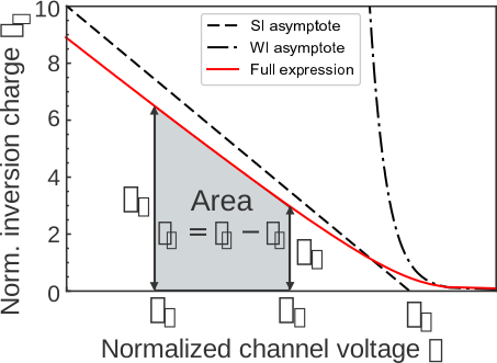
The inversion charge versus channel voltage was introduced in \(\eqref{eqn:4:qi_si}\) assuming that the transistor was biased in strong inversion. It can be shown that for a given gate voltage \(V_G\) (or its normalized form \(v_g \triangleq V_G/U_T\)) and therefore pinch-off voltage \(V_P\) (or its normalized form \(v_p \triangleq V_P/U_T\)), the normalized channel voltage \(v \triangleq V/U_T\) (which depends on the normalized position \(\xi\) along the channel) is given by [15] \[\begin{equation}\label{eqn:4:vp_v_qi} v_p-v(\xi) = \ln[q_i(\xi)] + 2q_i(\xi) \quad \textsf{for $0 \leq \xi \leq 1$}, \end{equation}\] which is valid all along the channel, from source to drain (assuming that \(V_D < V_P\), i.e. no saturation at the drain side of the channel). The normalized inversion charge \(q_i\) is plotted versus the channel voltage \(v\) in Figure 9 for a given gate and pinch-off voltage such that the transistor is biased in moderate inversion. The general expression \(\eqref{eqn:4:vp_v_qi}\) is compared to the strong and weak inversion asymptotes. We see that \(q_i\) no longer crosses the x-axis at \(v_p\) as the SI asymptotes does but decays exponentially to zero. We also see that the actual inversion charge is slightly smaller than the SI asymptote.
Note that \(\eqref{eqn:4:vp_v_qi}\) is also valid at the source and drain sides of the channel resulting in [15] \[\begin{align} v_p-v_s &= \ln(q_s) + 2q_s,\label{eqn:4:vp_vs_qs}\\ v_p-v_d &= \ln(q_d) + 2q_d,\label{eqn:4:vp_vd_qd} \end{align}\] where \(q_s\) and \(q_d\) correspond to the normalized inversion charges at the source and drain \[\begin{align}\label{eqn:4:qs_qd_def} q_s &\triangleq q_i(\xi=0) = \frac{Q_i(x=0)}{Q_{spec}},\\ q_d &\triangleq q_i(\xi=1) = \frac{Q_i(x=L)}{Q_{spec}}. \end{align}\] We will see that \(q_s\) and \(q_d\) are fundamental variables in the EKV charge-based model. Indeed, almost any characteristic of the intrinsic transistor can be expressed in terms of \(q_s\) and \(q_d\). As a first example, we now will derive an expression of the drain current in terms of \(q_s\) and \(q_d\) that is valid in all modes of operation.
4.2.7 Drain current in all modes of operation
The drain current given by \(\eqref{eqn:4:id_di_dv_dx}\) can be written in normalized form as \[\begin{equation}\label{eqn:4:id_qi_dvdxi} i_d \triangleq \frac{I_D}{I_{spec}} = q_i\,\frac{d v}{d \xi}. \end{equation}\] The current still corresponds to the area below the \(q_i\) curve comprised between \(v_s\) and \(v_d\) as shown in Figure 9 and can still be decomposed into the difference between a forward \(i_f\) and a reverse \(i_r\) normalized current \[\begin{equation} i_d = i_f - i_r, \end{equation}\] but the integration needs now to be performed from \(v_s\), respectively \(v_d\) to \(+\infty\) in order to include moderate and weak inversion \[\begin{align} i_f &\triangleq \frac{I_F}{I_{spec}} = \int_{v_s}^{+\infty} q_i \cdot dv,\label{eqn:4:if_v}\\ i_r &\triangleq \frac{I_R}{I_{spec}} = \int_{v_d}^{+\infty} q_i \cdot dv.\label{eqn:4:ir_v} \end{align}\]
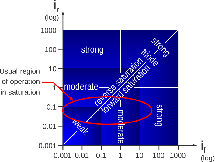
The normalized forward and reverse currents can be used to define the various modes of operation of the transistor including the moderate inversion. It is shown in Figure 10. Except for switches which operate along the \(45^{\circ}\) line, most of the transistors of analog circuits are biased in saturation with \(i_r \ll 1\), corresponding to the red ovale in Figure 10.
Instead of performing the integration in the voltage domain as done in \(\eqref{eqn:4:if_v}\) and \(\eqref{eqn:4:ir_v}\), we can use \(\eqref{eqn:4:vp_v_qi}\) to express the channel voltage in terms of the inversion charge as \[\begin{equation} v = v_p - 2q_i - \ln(q_i), \end{equation}\] from which, assuming a constant gate and hence pinch-off voltage, we get \[\begin{equation}\label{eqn:4:dv_dqi} dv = -\left(2 + \frac{1}{q_i}\right)\,dq_i. \end{equation}\] Replacing \(\eqref{eqn:4:dv_dqi}\) in \(\eqref{eqn:4:id_qi_dvdxi}\) results in \[\begin{equation}\label{eqn:4:id_qi} i_d = -(2q_i+1) \cdot \frac{dq_i}{d\xi}. \end{equation}\] The drain current now only depends on the inversion charge and its derivative along the channel. Integrating \(\eqref{eqn:4:id_qi}\), we get \[\begin{align} i_f &= \int_{0}^{q_s} (2q_i+1) \cdot dq_i = q_s^2+q_s = q_s\,(q_s+1),\label{eqn:4:if_qs}\\ i_r &= \int_{0}^{q_d} (2q_i+1) \cdot dq_i = q_d^2+q_d = q_d\,(q_d+1),\label{eqn:4:ir_qd} \end{align}\] where we have swapped the integration bounds due to the minus sign in \(\eqref{eqn:4:id_qi}\) and accounted for the fact that \(q_i(v \rightarrow +\infty) = 0\). We now have extremely simple expressions of the forward and reverse currents that depend only on \(q_s\) for \(i_f\) and \(q_d\) for \(i_r\).
The forward and reverse currents can be approximated by [15] \[\begin{equation} i_{f,r} = \begin{cases} q_{s,d} & \textsf{for $q_{s,d} \ll 1$ (weak inversion)},\\ q_{s,d}^2 & \textsf{for $q_{s,d} \gg 1$ (strong inversion)}. \end{cases} \end{equation}\]
In saturation, \(q_d \ll q_s\) making the reverse current \(i_r\) negligible compared to the forward current \(i_f\). The drain current is then simply equal to the forward current \[\begin{equation} i_d \cong i_f = q_s^2+q_s \quad \textsf{in forward saturation}. \end{equation}\]
The source and drain charges \(q_s\) and \(q_d\) can be expressed as a function of the forward and reverse currents \(i_f\) and \(i_r\) by solving \(\eqref{eqn:4:if_qs}\) and \(\eqref{eqn:4:ir_qd}\) for \(q_s\) and \(q_d\), respectively, resulting in [15] \[\begin{align} q_s &= \frac{\sqrt{4i_f+1}-1}{2} = \frac{2i_f}{\sqrt{4i_f+1}+1},\label{eqn:4:qs_if}\\ q_d &= \frac{\sqrt{4i_r+1}-1}{2} = \frac{2i_r}{\sqrt{4i_r+1}+1}.\label{eqn:4:qd_ir} \end{align}\] The normalized source and drain charges have the following asymptotes [15] \[\begin{equation} q_{s,d} = \begin{cases} i_{f,r} & \textsf{for $i_{f,r} \ll 1$ (weak inversion)},\\ \sqrt{i_{f,r}} & \textsf{for $i_{f,r} \gg 1$ (strong inversion)}. \end{cases} \end{equation}\]
Having the foward and reverse currents in terms of \(q_s\) and \(q_d\) is not very helpfull, because we still need to know \(q_s\) and \(q_d\) which are set by the terminal voltages according to \(\eqref{eqn:4:vp_vs_qs}\) and \(\eqref{eqn:4:vp_vd_qd}\). We can however replace \(q_s\) and \(q_d\) in \(\eqref{eqn:4:vp_vs_qs}\) and \(\eqref{eqn:4:vp_vd_qd}\) by \(\eqref{eqn:4:qs_if}\) and \(\eqref{eqn:4:qd_ir}\) resulting in two relations between the voltages and the currents [15] \[\begin{align} v_p-v_s &= \ln\left(\sqrt{4i_f+1}-1\right) + \sqrt{4i_f+1}-1-\ln(2),\label{eqn:4:vpvs_if}\\ v_p-v_d &= \ln\left(\sqrt{4i_r+1}-1\right) + \sqrt{4i_r+1}-1-\ln(2).\label{eqn:4:vpvd_ir} \end{align}\] We now have two relations of the terminal voltages in terms of the normalized currents which are valid in all regions of operation. However, we usually need an expression of the currents in terms of the terminal voltages. Unfortunately, \(\eqref{eqn:4:vpvs_if}\) and \(\eqref{eqn:4:vpvd_ir}\) cannot be inverted analytically to give an explicit closed-form expression of the drain current versus voltages valid in all regions of operation. However, \(\eqref{eqn:4:vpvs_if}\) and \(\eqref{eqn:4:vpvd_ir}\) can be inverted by means of the Lambert W-function \(W(z)\) which is defined as the function that satisfies the following equality [17], [18] \[\begin{equation}\label{eqn:4:lambert1} W(z) \cdot e^{W(z)} = z. \end{equation}\]
The voltage versus charge equation \(v=\ln(q)+2q\) can then be written as \[\begin{equation} 2q \cdot e^{2q} = 2e^v \end{equation}\] where \(q \triangleq q_s\) and \(v \triangleq v_p-v_s\) which can be solved for \(q\) using the Lambert W-function by setting \(z = 2e^v\) leading to \[\begin{equation} q(v) = \frac{1}{2} W(2e^v). \end{equation}\]
The Lambert W-function is available in the scipy Python library as lambertw and in Mathematica as the ProductLog[z] function.
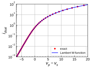
Figure 11 shows the normalized drain current in saturation \(i_{d_{sat}} = i_f\) versus \(v_p-v_s\). The exact curve is actually obtained by sweeping the current \(i_{d_{sat}}\) and calculating \(v_p-v_s\) using \(\eqref{eqn:4:vpvs_if}\). The Lambert W-function is obtained by taking the values of \(v_p-v_s\) obtained with \(\eqref{eqn:4:vpvs_if}\) and calculating \(i_{d_{sat}}\) using the Lambert W-function. Carefully looking at Figure 11 we see no difference. As shown in Figure 14, the relative error is negligible.
Although the Lambert W-function is available in math packages, it is not available in standard HDL used for implementing compact models such as Verilog-A for example. However, a simple approximation that does not require any iterations and which is offering a very good accuracy was proposed by Bucher and implemented in version 2.6 of the EKV compact model. The corresponding Python code is given below
def q_v(v):
  if v <= -15:
    q0=1/(2+exp(-v))
  else:
    if v <-0.35:
      z0=1.55+exp(-v)
    else:
      z0=2/(1.3+v-ln(v+1.6))
    z1=(2+z0)/(1+v+ln(z0))
    q0=(1+v+ln(z1))/(2+z1)
  return q0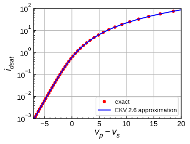
Figure 12 shows the normalized current calculated with the EKV 2.6 approximation which is compared to the exact result. Again, we see no difference. The relative error is larger than that of the Lambert-W function but remains negligible as show in Figure 14.
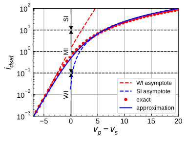
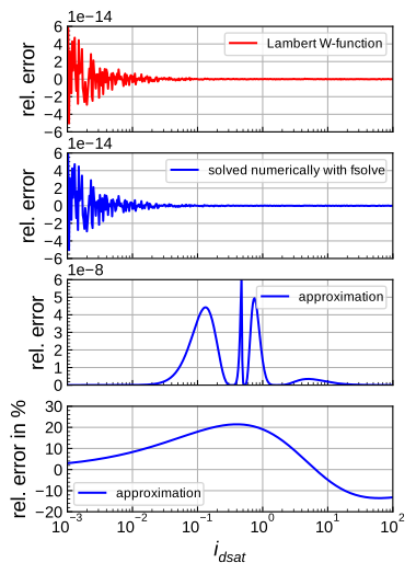
An alternative analytical expression of the current (and actually also the transconductance) that is valid in all regions of operation has been proposed by Cerveny and Vittoz [19], [15] \[\begin{align} v_p-v_s &= 2\ln\left[e^{\sqrt{i_f}}-1\right],\label{eqn:4:vps_if_vittoz}\\ v_p-v_d &= 2\ln\left[e^{\sqrt{i_r}}-1\right].\label{eqn:4:vpd_ir_vittoz} \end{align}\] The big advantage of \(\eqref{eqn:4:vps_if_vittoz}\) and \(\eqref{eqn:4:vpd_ir_vittoz}\) is that it can be inverted to express the currents in terms of the voltages as [19], [15] \[\begin{align} i_f &= \ln^2\left[1 + e^{\frac{v_p-v_s}{2}}\right],\label{eqn:4:if_vps_vittoz}\\ i_r &= \ln^2\left[1 + e^{\frac{v_p-v_d}{2}}\right].\label{eqn:4:ir_vpd_vittoz} \end{align}\] \(\eqref{eqn:4:if_vps_vittoz}\) is compared to the exact expression in Figure 13. We see that the approximation slightly underestimates the current in moderate inversion and overestimates it in strong inversion. The relative error is shown in the bottom plot of Figure 14. We see that it peaks to about \(+20\%\) in MI and \(-10\%\) in SI.
Sometimes it is useful to have the voltages referred to the source terminal instead of the bulk. For example, this is the case when analyzing the voltage follower, where the source terminal is the output and is floating. We start by expressing the saturation voltage \(V_P-V_S\) in terms of the gate-to-source voltage \(V_{GS}\) as \[\begin{equation}\label{eqn:4:VPS_VGS} V_P-V_S = \frac{V_G-V_{T0}}{n} - V_S = \frac{V_G-V_{T0} - n\,V_S}{n} =\frac{V_{GS}-V_T}{n}, \end{equation}\] where \(V_T\) is the threshold voltage for \(V_S > 0\) which increases with \(V_S\) according to \[\begin{equation}\label{eqn:4:VT} V_T \triangleq V_{T0} + (n-1) \cdot V_S. \end{equation}\]
The drain current in forward saturation (forward current) can now be written in terms of the \(V_{GS}\) voltage by replacing \(V_P-V_S\) by \(\eqref{eqn:4:VPS_VGS}\) in \(\eqref{eqn:4:if_vps_vittoz}\) resulting in \[\begin{equation}\label{eqn:4:id_vgs} i_d \cong i_f = \ln^2\left[1 + e^{\frac{V_{GS}-V_T}{2n\,U_T}}\right], \end{equation}\] which in weak inversion and saturation reduces to \[\begin{equation}\label{eqn:4:id_vgs_wi} i_d \cong e^{\frac{V_{GS}-V_T}{n\,U_T}}. \end{equation}\] In strong inversion, \(\eqref{eqn:4:id_vgs}\) reduces to \[\begin{equation}\label{eqn:4:id_vgs_si} i_d \cong \left(\frac{V_{GS}-V_T}{n\,U_T}\right)^2. \end{equation}\]
We can now check whether the charge-based model we have derived has the correct asymptotes in strong and in weak inversion.
4.2.8 Drain current in strong inversion
Assuming the transistor is biased in the linear region (i.e. neither the source nor the drain are pinched-off), in strong inversion we have \(q_s \gg 1\) and \(q_d \gg 1\) and similarly \(i_f \gg 1\) and \(i_r \gg 1\). The voltage versus charge equations \(\eqref{eqn:4:vp_vs_qs}\) and \(\eqref{eqn:4:vp_vd_qd}\) simplify to \[\begin{align} v_p-v_s &\cong 2q_s \cong 2\sqrt{i_f},\\ v_p-v_d &\cong 2q_d \cong 2\sqrt{i_r}, \end{align}\] which can now be inverted to express the current in terms of the voltages as \[\begin{align} i_f &\cong \left(\frac{v_p-v_s}{2}\right)^2 = \left(\frac{V_P-V_S}{2U_T}\right)^2,\\ i_r &\cong \left(\frac{v_p-v_d}{2}\right)^2 = \left(\frac{V_P-V_D}{2U_T}\right)^2. \end{align}\]
After denormalization we get \[\begin{equation} I_{F,R} = \begin{cases} \frac{n\beta}{2}(V_P-V_{S,D})^2 & \textsf{for $V_{S,D} \leq V_P$,}\\ 0 & \textsf{for $V_{S,D} > V_P$.} \end{cases} \end{equation}\]
Using the approximation of the pinch-off voltage \(V_P \cong (V_G-V_{T0})/n\) leads to \[\begin{equation} I_{F,R} = \begin{cases} \frac{\beta}{2n}(V_G-V_{T0}-nV_{S,D})^2 & \textsf{for $V_{S,D} \leq (V_G-V_{T0})/n$,}\\ 0 & \textsf{for $V_{S,D} > (V_{T0})/n$.} \end{cases} \end{equation}\]
The various expressions of the drain current in strong inversion are summarized in Table 2.
| Modes | \(I_D = I_F - I_R\) | Condition |
|---|---|---|
| Linear Region | \(n\,\beta\,\left(V_P-\frac{{V_D+V_S}}{{2}}\right)\,(V_D-V_S)\) | \(V_S<V_P\), \(V_D<V_P\) |
| \(\cong \beta\,\left[V_G-V_{{T0}}-\frac{{n}}{{2}}\,(V_D+V_S)\right]\,(V_D-V_S)\) | ||
| Forward saturation | \(\frac{{n\,\beta}}{{2}}\,(V_P-V_S)^2 \cong \frac{{\beta}}{{2n}}\,(V_G-V_{{T0}}-n\,V_S)^2\) | \(V_S<V_P\), \(V_D\geq V_P\) |
| Reverse saturation | \(-\frac{{n\,\beta}}{{2}}\,(V_P-V_D)^2 \cong -\frac{{\beta}}{{2n}}\,(V_G-V_{{T0}}-n\,V_D)^2\) | \(V_S\geq V_P\), \(V_D<V_P\) |
| Blocked | \(I_F=I_R=I_D=0\) | \(V_S\geq V_P\), \(V_D \geq V_P\) |
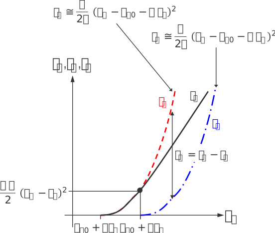
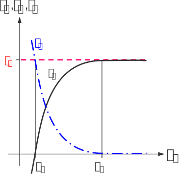
The transfer characteristic and output characteristics are plotted in Figure 15. Looking first at the transfer characteristic of Figure 15 (a), if we assume that \(V_S > 0\) and \(V_D > V_S\), when sweeping the gate voltage, the current remains zero until \(V_G\) reaches \(V_{T0}+n V_S\), point at which the transistor enters in forward saturation and the drain current becomes equal to the forward current since the drain is still pinched-off. The current then increases quadratically until \(V_G\) reaches \(V_{T0}+n V_D\), where the reverse current \(I_R\) starts to increase. The transistor then leaves the forward saturation region to enter into the linear region. In this region the current being the difference between the forward and reverse currents, which are both quadratic functions of the gate voltage, becomes a linear function of the gate voltage (this is the origin of the name of this region of operation).
We now look at the out charactersitic of Figure 15 (b). The foward current assuming a long-channel transistor does not depend on the drain voltage. So for a given gate and source voltage, \(I_F\) stays constant as shown by the dashed red curve in Figure 15 (b). On the other hand the reverse current decreases as we increase \(V_D\) until \(V_D\) reaches \(V_P\) above which it stays at zero. as shown by the dashed-dotted blue curve in Figure 15 (b). The drain current being the difference between \(I_F\) and \(I_R\), it increases until \(V_D\) reaches \(V_P\) where it saturates to \(I_F\). Notice that for \(V_D < V_S\), the drain current becomes negative because the reverse current becomes larger than the forward current.
4.2.9 Drain current in weak inversion
In weak inversion, we have \(q_s \ll 1\) and \(q_d \ll 1\) and similarly \(i_f \ll 1\) and \(i_r \ll 1\) and the voltage versus charge equations \(\eqref{eqn:4:vp_vs_qs}\) and \(\eqref{eqn:4:vp_vd_qd}\) can be approximated by \[\begin{align} v_p-v_s &\cong \ln\left(\sqrt{i_f+\frac{1}{4}}-\frac{1}{2}\right) \cong \ln\left(i_f\right),\\ v_p-v_d &\cong \ln\left(\sqrt{i_r+\frac{1}{4}}-\frac{1}{2}\right) \cong \ln\left(i_r\right). \end{align}\] which can now be inverted to express the current in terms of voltages as \[\begin{align} i_f &\cong e^{v_p-v_s},\\ i_r &\cong e^{v_p-v_d}. \end{align}\] If we denormalize the currents and voltages, we get \[\begin{align} I_F = I_{spec} \cdot e^{\frac{V_P-V_S}{U_T}} = I_{spec} \cdot e^{\frac{V_G-V_{T0}-n\,V_S}{n\,U_T}} = I_{D0} \cdot e^{\frac{V_G-n\,V_S}{n\,U_T}},\\ I_R = I_{spec} \cdot e^{\frac{V_P-V_D}{U_T}} = I_{spec} \cdot e^{\frac{V_G-V_{T0}-n\,V_D}{n\,U_T}} = I_{D0} \cdot e^{\frac{V_G-n\,V_D}{n\,U_T}}. \end{align}\] where \(I_{D0}\) is the leakage current, that means the current that flows in saturation when the gate voltage is set to zero \[\begin{equation}\label{eqn:4:ID0} I_{D0} = I_{spec} \cdot e^{-\frac{V_{T0}}{n\,U_T}}. \end{equation}\]
The expressions of the drain current in weak inversion are summarized in Table 3.
| Modes | \(I_D = I_F - I_R\) | Condition |
|---|---|---|
| Linear Region | \(I_{{spec}}\,e^{{\frac{{V_P}}{{U_T}}}}\left[e^{{-\frac{{V_S}}{{U_T}}}} - e^{{-\frac{{V_D}}{{U_T}}}}\right]\) | \(V_S>V_P\), \(V_D>V_P\) |
| \(\cong I_{{D0}}\,e^{{\frac{{V_G}}{{n\,U_T}}}}\left[e^{{-\frac{{V_S}}{{U_T}}}} - e^{{-\frac{{V_D}}{{U_T}}}}\right]\) | ||
| Forward saturation | \(I_{{spec}}\,e^{{\frac{{V_P-V_S}}{{U_T}}}} \cong I_{{D0}}\,e^{{\frac{{V_G-n\,V_S}}{{n\,U_T}}}}\) | \(V_D-V_S\gg U_T\) |
| Reverse saturation | \(-I_{{spec}}\,e^{{\frac{{V_P-V_D}}{{U_T}}}} \cong -I_{{D0}}\,e^{{\frac{{V_G-n\,V_D}}{{n\,U_T}}}}\) | \(V_S-V_D\gg U_T\) |
| Blocked | \(I_F=I_R=I_D=0\) | \(V_S\gg U_T\), \(V_D \gg U_T\) or \(V_D=V_S\) |
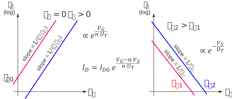
The transfer characteristics \(I_D\)-\(V_G\) are plotted in Figure 16 with a logarithmic y-axis. The slope of the I-V characteristic is equal to \(1/(n\,U_T)\). The leakage current \(I_{D0}\) corresponds to the intersection of the I-V characteristic for \(V_S=0\) and the y-axis. Note that \(I_{D0}\) is very sensitive to the threshold voltage since it depends exponentially on it as shown in \(\eqref{eqn:4:ID0}\). The leakage current therefore increases exponentially when the threshold is reduced. This is the reason why the threshold voltage could not be scaled in the same way than the supply voltage in order to avoid prohibitive leakage current. This resulted in a reduction of the overdrive voltage \(V_G-V_{T0}\) and hence a move of the operating point from SI towards MI.
The transfer characteristics \(I_D\)-\(V_S\) are plotted in Figure 16 with a logarithmic y-axis for two different values of the gate voltage. We see that the current is decreasing exponentially with \(V_S\) with an ideal slope equal to \(1/U_T\).
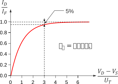
The output characteristic \(I_D\)-\(V_D\) is plotted in Figure 17 where the drain current is normalized to the forward current resulting in \[\begin{equation} \frac{I_D}{I_F} = \frac{I_F-I_R}{I_F} = 1 - \frac{I_R}{I_F} = 1 - e^{-\frac{V_D-V_S}{U_T}}. \end{equation}\] We see that, contrary to strong inversion, we cannot clearly identify a saturation voltage, namely a voltage above which the current saturates to a constant value. In weak inversion, the saturation current is only reached for \(V_D-V_S \gg U_T\) (formally only for \(V_D-V_S \; \rightarrow \; \infty\)). However, because of the exponential dependance, the current quickly reaches the maximum current. A saturation voltage can be defined by the difference between the actual curve and the asymptotic value of the current. If this difference is set to 5%, the saturation voltage is only about \(3U_T \cong 80\;mV\).
Important
The saturation voltage in weak inversion is the lowest saturation voltage for a given device. This is the reason why weak inversion is interesting for low-voltage operation. Note also that, contrary to strong inversion, the saturation voltage in weak inversion is independent of the threshold voltage.
4.2.10 Subthreshold slope
The subthreshold slope or gate swing is defined as the increase of gate voltage (in mV) required for the drain current to increase by one order of magnitude (10x) \[\begin{equation} \triangle V_G = n\,U_T \ln10 = 2.3 n\,U_T = 2.3 n \frac{k_B\,T}{q} \end{equation}\] which is measured in mV per decade with \(U_T\) expressed in mV. At room temperature it is typically equal to 90 mV/dec. It can be compared to the 60 mV/dec obtained for a bipolar transistor or a fully depleted SOI MOS device for which the slope factor can be considered ideal (\(n=1\)). It also scales with temperature (at least down to about 50 K).
4.2.11 The inversion coefficient

The overdrive voltage \(V_G-V_{T0}\) (or \(V_G-V_T\)) which has traditionally been used as the main design parameter for setting the bias point of transistors operating in strong inversion is no more suited when moving to moderate and weak inversion. Indeed, it becomes zero or even negative which is not very convenient. We instead propose to use the inversion coefficient \(IC\) which basically defines the level of inversion of the transistor and is formally defined as the maximum of the normalized forward or reverse current \(IC \triangleq \max(i_f,i_r)\). Since most of the time the transistor is biased in forward saturation then \(IC\) is defined as [15], [6], [7], [8], [9] \[\begin{equation}\label{eqn:4:IC_def} IC \triangleq \frac{\left.I_D\right|_{saturation}}{I_{spec}}, \end{equation}\] where the normalizing factor \(I_{spec}\) is called the specific current, and is defined as [15], [6], [7], [8], [9] \[\begin{equation}\label{eqn:4:ispec_def} \boxed{ I_{spec} \triangleq I_{spec\Box} \cdot \frac{W}{L}, } \end{equation}\] with \[\begin{equation}\label{eqn:4:ispecsq_def} \boxed{ I_{spec\Box} \triangleq 2n \mu C_{ox} U_T^2. } \end{equation}\] In a given technology, the specific currents per square \(I_{spec\Box}\), one for each transistor type (n- and p-channel), are the most fundamental parameters for the designer.
Using \(IC\), the different regions of operation of a MOSFET can be classified as illustrated in Figure 18 and defined below [15], [6], [7], [8], [9] \[\begin{align} &IC \leq 0.1 &&\textsf{weak inversion (WI)},\\ 0.1 <& IC \leq 10 &&\textsf{moderate inversion (MI)},\\ 10 <& IC &&\textsf{strong inversion (SI).} \end{align}\]
4.2.12 Saturation voltage
The saturation voltage is the drain-to-source voltage \(V_{DS}\) above which the drain current saturates to the foward current \(I_F\) [15]. In strong inversion, the saturation voltage corresponds to the pinch-off voltage \(V_P\) and hence the drain-to-source saturation voltage is given by \(V_{DSsat} = V_P-V_S\) [15]. In weak inversion, we cannot define a drain-to-source saturation voltage because the drain current actually never reaches \(I_F\) but tends asymptotically to it. We cannot use \(V_P-V_S\) because it becomes zero in moderate inversion or negative in weak inversion as shown in Figure 19.
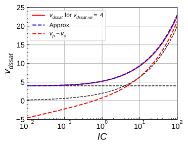
From \(\eqref{eqn:4:vp_vs_qs}\) and \(\eqref{eqn:4:vp_vd_qd}\) we can express the normalized drain-to-source voltage \(v_{ds}\) as a function of the normalized charges at the source \(q_s\) and drain \(q_d\) as \[\begin{equation}\label{eqn:4:vds_qs_qd} v_{ds} = v_d-v_s = 2(q_s-q_d) + \ln\left(\frac{q_s}{q_d}\right) = 2 q_s\,\left(1-\frac{q_d}{q_s}\right) - \ln\left(\frac{q_d}{q_s}\right). \end{equation}\]
We can define a saturation voltage using the \(q_d/q_s\) ratio (or its inverse the \(q_s/q_d\) ratio) as a criterium to define the saturation voltage \[\begin{equation}\label{eqn:4:vdssat_r} v_{dssat} = 2 q_s\,(1-r)-\ln(r), \end{equation}\] where \(r=q_d/q_s\) and \(q_s\) depends on the inversion coefficient according to \(\eqref{eqn:4:qs_if}\) \[\begin{equation} q_s = \frac{\sqrt{4 IC+1}-1}{2}. \end{equation}\]
In weak inversion, the ratio \(r\) can be expressed as \[\begin{equation} r = \frac{q_d}{q_s} \cong \frac{i_r}{i_f} \cong e^{-v_{dssat,wi}} \end{equation}\] We can therefore also express the drain-to-source saturation voltage in terms of its value in weak inversion \(v_{dssatwi}\) as \[\begin{equation}\label{eqn:4:vdssat_vdssatwi} v_{dssat} = 2 q_s\,\left(1-e^{-v_{dssatwi}}\right)+v_{dssatwi}. \end{equation}\] If we choose \(v_{dssat,wi} =\) 4, \(\eqref{eqn:4:vdssat_vdssatwi}\) can be approximated by \[\begin{equation}\label{eqn:4:vdssat_approx} v_{dssat} = 2 q_s\,\left(1-e^{-4}\right)+4 \cong \sqrt{4 IC+1} + 3 \end{equation}\] Equations \(\eqref{eqn:4:vdssat_vdssatwi}\) and its approximation \(\eqref{eqn:4:vdssat_approx}\) are plotted versus the inversion coefficient \(IC\) in Figure 19. We see an almost perfect fit.
Notebook: Saturation voltage
This Notebook gives a detailed derivation of the saturation voltage which is valid in all modes of operation from weak to strong inversion.
4.3 The small-signal model
4.3.1 The low-frequency small-signal model
4.3.1.1 Small-signal schematic of the bulk transistor
The small-signal model is essential for the linear analysis of simple circuits such amplifiers. It is based on the small-signal model of the transistor which is presented in this section.
Since the bulk MOS transistor has four terminals and three control voltages, the gate voltage \(V_G\), the source voltage \(V_S\) and the drain voltage \(V_D\), we can define three different transconductances. The drain current increment \(\Delta I_D\) due to an increment of the terminal voltages around an operating point is given by \[\begin{equation}\label{eqn:4:deltaID} \begin{split} \Delta I_D &= G_m \cdot \Delta V_G - (G_{ms}+G_{ds}) \cdot \Delta V_S + (G_{md}+G_{ds}) \cdot \Delta V_D\\ &= G_m \cdot \Delta V_G - G_{ms} \cdot \Delta V_S + G_{md} \cdot \Delta V_D + G_{ds} \cdot \Delta V_{DS}, \end{split} \end{equation}\] where \[\begin{align}\label{eqn:4:Gmx} &G_m = \left.\frac{\partial I_D}{\partial V_G}\right|_{\text{op}},\\ &G_{ms} + G_{ds} = \left.-\frac{\partial I_D}{\partial V_S}\right|_{\text{op}},\\ &G_{md} + G_{ds} = \left.\frac{\partial I_D}{\partial V_D}\right|_{\text{op}}. \end{align}\] where op corresponds to the operating point set by the three DC voltages applied at the gate, source and drain. \(G_m\), \(G_{ms}\) and \(G_{md}\) are the gate, source and drain transconductances, respectively and \(G_{ds}\) is the output conductance typically due to channel-length modulation (CLM) and drain-induced barrier lowering (DIBL). Note the negative sign of the second term in \(\eqref{eqn:4:deltaID}\) which is due to the fact that increasing the source voltage makes the current decrease. It has thus been chosen to get a positive source transconductance.
Note
Note that \(G_{md}\) is not equal to \(G_{ds}\). \(G_{md}\) is the transconductance from the drain inherent to the transistor effect while the conductance is due to short-channel effects such as channel-length modulation (CLM) and drain-induced barrier lowering (DIBL). Note that for long-channel transistors, \(G_{ds} \ll G_{ms}\) and the output conductance can usually be neglected.
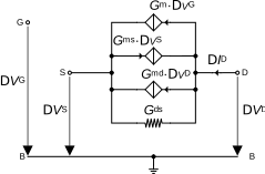
The equivalent low-frequency small-signal circuit is shown in Figure 20 and includes three voltage-controlled current sources (VCCS), each representing one of the transconductance in addition to the output conductance.
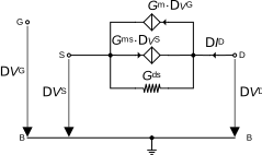
In forward saturation, for a long channel transistor, the drain voltage has no influence on the drain current except through the output conductance \(G_{ds}\) and hence \(G_{md}=0\). The drain current increment \(\eqref{eqn:4:deltaID}\) then reduces to \[\begin{equation}\label{eqn:4:deltaID_sat} \Delta I_D = G_m \cdot \Delta V_G - G_{ms} \cdot \Delta V_S + G_{ds} \cdot \Delta V_{DS} \end{equation}\] and the equivalent small-signal circuit simplifies to the one shown in Figure 21. Note that \(G_{ms}\) should not be confused with the bulk transconductance \(G_{mb}\). In forward saturation, the transconductances of a source referenced model are related to the transconductances of a bulk referenced model according to \[\begin{align} &\left.G_m\right|_{\text{source}} = \left.G_m\right|_{\text{bulk}} = G_m,\\ &\left.G_{mb}\right|_{\text{source}} = \left.G_{ms}\right|_{\text{bulk}} - \left.G_m\right|_{\text{bulk}} = (n-1)\,G_m,\\ &\left.G_{ds}\right|_{\text{source}} = \left.G_{ds}\right|_{\text{bulk}} = G_{ds}. \end{align}\] where the relation \(G_{ms}=n \cdot G_m\) that will be discussed later has been used.
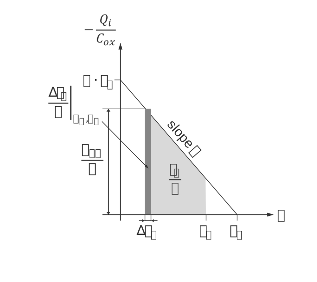
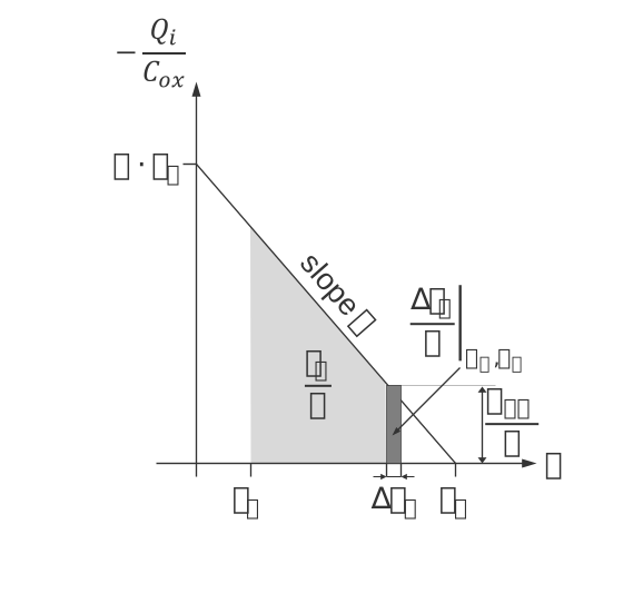
The gate, source and drain transconductances are related to each other by the source and drain charges. Indeed, looking again at the \(-Q_i/C_{ox}\) versus \(V\) plot shown in Figure 22 and remembering that the area below the curve comprised between \(V_S\) and \(V_D\) corresponds to \(I_D/\beta\), we first make the following experience illustrated in Figure 22 (a). Let’s increase the source voltage by \(\Delta V_S\). This will reduce the drain current by \(\Delta I_D\) which corresponds to the area of the dark grey rectangle (actually \(\Delta I_D/\beta\)). Since by definition \(|\Delta I_D| = G_{ms} \cdot \Delta V_S\), the height of the rectangle is therefore equal to \(G_{ms}/\beta\). But the height of this rectangle also corresponds to the value of the inversion charge (normalized to \(C_{ox}\)) at the source. The source transconductance is therefore proportional to the inversion charge evaluated at the source [15] \[\begin{equation}\label{eqn:4:gms_qs} G_{ms} = \beta \cdot \left.\frac{-Q_i}{C_{ox}}\right|_{V=V_S} = G_{spec} \cdot q_s, \end{equation}\] where \(G_{spec} = I_{spec}/U_T\). In a similar way, we can increase the drain voltage by \(\Delta V_D\) assuming the transistor is biased in the linear region, which results in an increase of the drain current corresponding to the dark grey rectangle. For similar reasons found for the source transconductance, the drain transconductance is proportional to the inversion charge but now evaluated at the drain [15] \[\begin{equation}\label{eqn:4:gmd_qd} G_{md} = \beta \cdot \left.\frac{-Q_i}{C_{ox}}\right|_{V=V_D} = G_{spec} \cdot q_d. \end{equation}\]
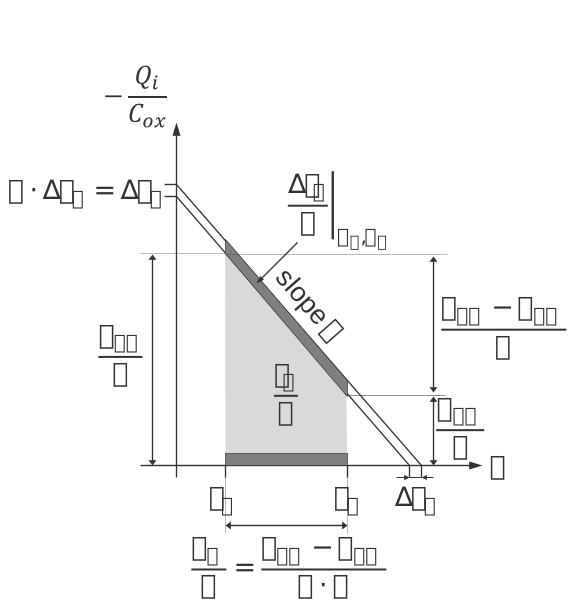
If we now increase the gate voltage by \(\Delta V_G\) as illustrated in Figure 22 (c), the whole curve moves up by \(n \cdot \Delta V_P \cong \Delta V_G\) since \(V_P \cong (V_G - V_{T0})/n\) and \(-Q_i/C_{ox}\) is given by \(\eqref{eqn:4:qi_si}\). The current increment is then corresponding to the top dark grey area which can be shown to be equal to the bottom dark grey rectangle having a height \(\Delta V_G\). The length of this rectangle then corresponds to the gate transconductance \(G_m/\beta\). It is also equal to the difference \((G_{ms}-G_{md})/\beta\) divided by the slope \(n\). We therefore have the following relation between \(G_m\), \(G_{ms}\) and \(G_{md}\) [15] \[\begin{equation}\label{eqn:4:gm_gms_gmd} G_m = \frac{G_{ms}-G_{md}}{n}. \end{equation}\] Using \(\eqref{eqn:4:gms_qs}\) and \(\eqref{eqn:4:gmd_qd}\), \(\eqref{eqn:4:gm_gms_gmd}\) writes [15] \[\begin{equation} G_m = G_{spec} \cdot \frac{q_s - q_d}{n}. \end{equation}\]
The fundamental relations \(\eqref{eqn:4:gms_qs}\), \(\eqref{eqn:4:gmd_qd}\) and \(\eqref{eqn:4:gm_gms_gmd}\) have been derived from simple geometrical considerations in strong inversion. However it can be shown that they are valid in all modes of inversion. Indeed, differentiating \(\eqref{eqn:4:id}\) with respect to \(V_S\) and \(V_D\) results in [15] \[\begin{align} &G_{ms} = -\frac{\partial I_D}{\partial V_S} = -\frac{\partial I_F}{\partial V_S} = \beta \cdot \left.\frac{-Q_i}{C_{ox}}\right|_{V=V_S} = \beta \cdot \frac{-Q_i(x=0)}{C_{ox}} = G_{spec} \cdot q_s,\\ &G_{md} = \frac{\partial I_D}{\partial V_D} = -\frac{\partial I_R}{\partial V_D} = \beta \cdot \left.\frac{-Q_i}{C_{ox}}\right|_{V=V_D} = \beta \cdot \frac{-Q_i(x=L)}{C_{ox}} = G_{spec} \cdot q_d. \end{align}\] Finally, the gate transconductance is given by [15] \[\begin{equation}\label{eqn:4:Gm_IF_IR} G_m = \frac{\partial I_D}{\partial V_G} = \frac{\partial I_D}{\partial V_P} \cdot \frac{dV_P}{dV_G} = \frac{1}{n} \cdot \left(\frac{\partial I_F}{\partial V_P} - \frac{\partial I_R}{\partial V_P}\right) \end{equation}\] since \[\begin{equation} \frac{dV_P}{dV_G} = \frac{1}{n}. \end{equation}\] Now, since the forward current \(I_F\) is a function of \(V_P-V_S\), differentiating \(I_F\) with respect to \(V_P\) is the same as differentiating \(I_F\) with respect to \(-V_S\) and hence \[\begin{equation}\label{eqn:4:dIF_dVP} \frac{\partial I_F}{\partial V_P} = - \frac{\partial I_F}{\partial V_S} = G_{ms}. \end{equation}\] Similarly, since the reverse current \(I_R\) is a function of \(V_P-V_D\), differentiating \(I_R\) with respect to \(V_P\) is the same as differentiating \(I_R\) with respect to \(-V_D\) and hence \[\begin{equation}\label{eqn:4:dIR_dVP} \frac{\partial I_R}{\partial V_P} = - \frac{\partial I_R}{\partial V_D} = G_{md}. \end{equation}\] From \(\eqref{eqn:4:Gm_IF_IR}\), \(\eqref{eqn:4:dIF_dVP}\) and \(\eqref{eqn:4:dIR_dVP}\), we finally get \(\eqref{eqn:4:gm_gms_gmd}\). Note that the above derivation has been made without any assumption on the transistor mode of operation (except that it is a long-channel transistor biased in inversion).
In forward saturation, we have \(G_{md}=0\) and hence, \(\eqref{eqn:4:gm_gms_gmd}\) simplifies to \[\begin{equation}\label{eqn:4:Gm_Gms} G_m = \frac{G_{ms}}{n}. \end{equation}\] Equation \(\eqref{eqn:4:Gm_Gms}\) states that the transconductance from the gate is \(n\) times smaller than the transconductance from the source. This means that for current-efficiency we should always control the transistor from the source. However, the reason we control it from the gate is that the impedance seen at the source is low (actually equal to \(1/G_{ms}\)) whereas the impedance seen at the gate is very high.
4.3.1.2 Small-signal Schematic of the FDSOI Transistor
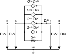
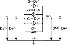
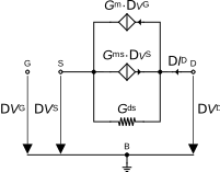
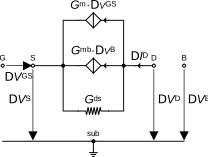
Note that since an FDSOI device is a four terminal device, there is an additional transconductance \(G_{mb}\) coming from the back gate. There are therefore 4 VCCS as shown in Figure 23 (a). The front- and the back-gate transconductances are then given by \[\begin{align} &G_m = \frac{G_{ms}-G_{md}}{n_f},\\ &G_{mb} = \frac{G_{ms}-G_{md}}{n_b}, \end{align}\] where \(n_f\) and \(n_b\) are the front- and back-gate slope factors, respectively. The subthreshold slope factors of the front- and back-gate \(n_f\) and \(n_b\) are coupled and are therefore bias-dependent typically depending on the gate voltage difference \(V_G-V_B\) [20]. For a long-channel transistor, the front-gate slope factor \(n_f\) is very close to one, typically ranging between \(1.04 < n_f < 1.11\), whereas the back-gate slope factor \(n_b\) is approximately given by \[\begin{equation} n_b \cong \frac{n_f}{n_f - 1} \end{equation}\] and typically ranges between \(10 < n_b < 25\). As expected, this reflects the fact that the transconductance from the back-gate is much less efficient that the transconductance from the front-gate.
In saturation, \(G_{md} = 0\) and the small-signal circuit reduces to that shown in Figure 23 (b) with \[\begin{align} &G_m = \frac{G_{ms}}{n_f},\\ &G_{mb} = \frac{G_{ms}}{n_b}. \end{align}\]
Of course when the back gate is connected to a DC bias voltage then \(G_{mb}=0\) and the small-signal schematic in saturation reduces to the equivalent circuit shown in Figure 23 (c), which is identical to the small-signal schematic of the bulk MOSFET shown in Figure 21. Finally, for a long-channel FDSOI device, the front-gate slope factor can be approximated by \(n_f \cong 1\). The gate and source transconductances are then equal and can be merged into a single transconductance \(G_m\) but now controlled by \(V_{GS}\). The equivalent schematic in saturation including the back-gate transconductance is shown in Figure 23 (d).
4.3.1.3 Transconductances in strong inversion
The transconductance values in strong inversion can be derived from the expression of the forward and reverse current [15] \[\begin{align} &G_{ms} = n \beta (V_P-V_S) = \sqrt{2n \beta I_F} = \frac{2 I_F}{V_P-V_S},\\ &G_{md} = n \beta (V_P-V_D) = \sqrt{2n \beta I_R} = \frac{2 I_R}{V_P-V_D},\\ &G_m = \frac{G_{ms}-G_{md}}{n} = \beta V_{DS} = \sqrt{\frac{2\beta}{n}} \cdot \left(\sqrt{I_F}-\sqrt{I_R}\right). \end{align}\]
In saturation, \(I_R \cong 0\) and \(I_D \cong I_F\) and the above expressions reduce to [15] \[\begin{align}\label{eqn:4:Gm_Gms_SI} &G_{ms} = n \beta (V_P-V_S) = \sqrt{2n \beta I_D} = \frac{2 I_D}{V_P-V_S},\\ &G_{md} \cong 0,\\ &G_m = \frac{G_{ms}}{n} = \beta (V_P-V_S) = \sqrt{\frac{2\beta I_D}{n}} = \frac{2 I_D}{n(V_P-V_S)}. \end{align}\]
From \(\eqref{eqn:4:Gm_Gms_SI}\) we see that in strong inversion and saturation, \(G_m\) depends on two design parameters: either \(\beta\) and \(V_P-V_S\) or \(\beta\) and \(I_D\) or \(I_D\) and \(V_P-V_S\).
4.3.1.4 Transconductances in weak inversion
In weak inversion, the transconductances are related to the forward and reverse currents according to [15] \[\begin{align} &G_{ms} = \frac{I_F}{U_T},\\ &G_{md} = \frac{I_R}{U_T},\\ &G_m = \frac{G_{ms}-G_{md}}{n} = \frac{I_F-I_R}{n\,U_T} = \frac{I_D}{n\,U_T}. \end{align}\]
In saturation, \(I_R \ll I_F\) and \(I_D \cong I_F\) and the above expressions reduce to [15] \[\begin{align} &G_{ms} = \frac{I_D}{U_T},\\ &G_{md} \cong 0,\\ &G_m = \frac{G_{ms}}{n} = \frac{I_D}{n\,U_T}. \end{align}\]
4.3.1.5 Transconductances in all regions of inversion
One of the main reason to choose a charge-based model instead of a surface potential-based model, is the fundamental link that exists between the inversion charge and the transconductance which is the most important parameter for analog circuit design. Since we have a relation between the source (drain) charge and the forward (reverse) current (c.f. \(\eqref{eqn:4:qs_if}\) and \(\eqref{eqn:4:qd_ir}\)), and since the source (drain) transconductance is proportional to the source (drain) charge (c.f. \(\eqref{eqn:4:gms_qs}\) and \(\eqref{eqn:4:gmd_qd}\)), we can derive an expression of the transconductance as a function of the current that is valid in all regions of inversion [15] \[\begin{align} &G_{ms} = G_{spec} \cdot q_s = G_{spec} \cdot g_{ms}(i_f),\\ &G_{md} = G_{spec} \cdot q_d = G_{spec} \cdot g_{ms}(i_r),\\ &G_m = \frac{G_{ms}-G_{md}}{n} = G_{spec} \cdot \frac{g_{ms}(i_f)-g_{ms}(i_r)}{n}. \end{align}\] with \(g_{ms}\) being the normalized source transconductance given by \[\begin{equation}\label{eqn:4:gms_def} \boxed{ g_{ms}(IC) \triangleq \frac{G_{ms}}{G_{spec}} = \frac{\sqrt{4 IC+1}-1}{2} = \frac{2 IC}{\sqrt{4 IC+1}+1}. } \end{equation}\] Note that the above expressions are valid in all regions of inversion.
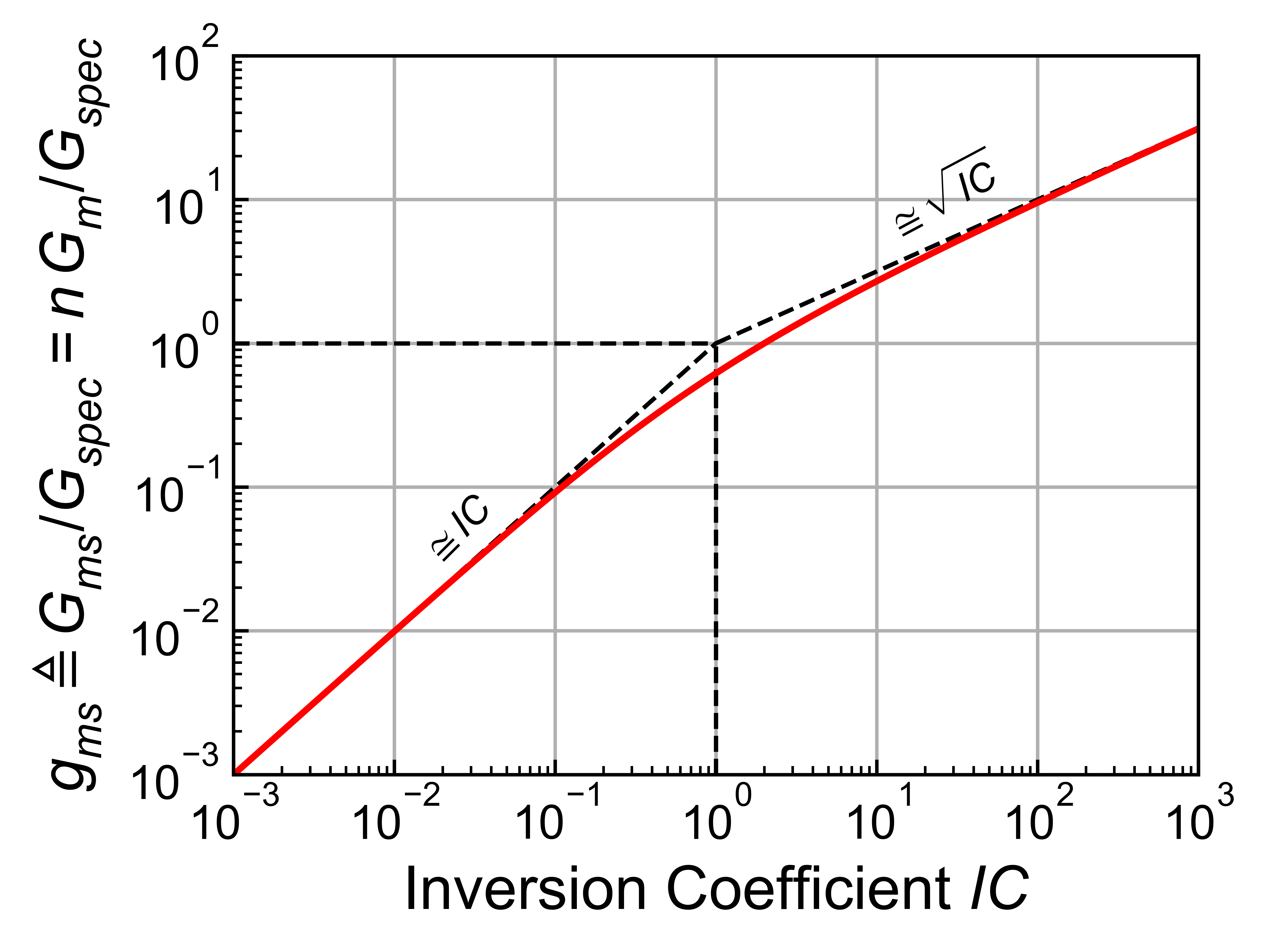
The function \(g_{ms}(IC)\) defined in \(\eqref{eqn:4:gms_def}\) is plotted versus the inversion coefficient \(IC\) in Figure 24. For \(IC \ll 1\), \(g_{ms}\) is equal to \(IC\), whereas for \(1 \ll IC\), \(g_{ms}\) reduces to \(\sqrt{IC}\).
4.3.1.6 Current efficiency or \(G_m/I_D\) ratio (long-channel)
The transconductance efficiency \(G_m/I_D\), sometimes also called the current-efficiency, is one of the most important figures-of-merit (FoM) for low-power analog circuit design.
Important
The transconductance efficiency \(G_m/I_D\) is a measure of how much transconductance is produced for a given bias current and is a function of \(IC\) only.
As will be shown later, the transconductance efficiency (or its inverse) appears in many expressions related to the optimization of analog circuits. The transconductance in saturation is related to the inversion coefficient (or normalized current) according to \[\begin{equation} G_{ms} = n \, G_m = G_{spec} \cdot g_{ms}(IC) \end{equation}\] where \(g_{ms}\) is given by \(\eqref{eqn:4:gms_def}\).
The normalized current-efficiency is then given by dividing the actual transconductance by the transconductance obtained in weak inversion \(I_D/U_T\), resulting in \[\begin{equation}\label{eqn:4:gmsid_long} \boxed{ \frac{G_{ms} \cdot U_T}{I_D} = \frac{G_m \cdot n\,U_T}{I_D} = \frac{\sqrt{4IC+1}-1}{2IC} = \frac{2}{\sqrt{4IC+1}+1}, } \end{equation}\] which has the following asymptotes \[\begin{equation}\label{eqn:4:gmsid_asym} \frac{G_{ms} \cdot U_T}{I_D} = \frac{G_m \cdot n\,U_T}{I_D} = \begin{cases} 1 & \textsf{in weak inversion and saturation,}\\ \frac{1}{\sqrt{IC}} & \textsf{in strong inversion and saturation.} \end{cases} \end{equation}\]
The current-efficiency is therefore maximum in weak inversion which means that for a given current budget it is better to bias the transistor in weak inversion to get the maximum transconductance. Or alternatively, to achieve a given transconductance biasing the transistor in weak inversion saves current.
Important
Biasing the transistor in weak inversion provides the highest transconductance for a given current budget. However, this does not mean that the maximum transconductance is achieved in weak inversion. As shown in Figure 24, the transconductance always increases when increasing the inversion coefficient.
During the design it is often required to find the inversion coefficient corresponding to a required transconductance for a given bias current. In order to do this we can invert \(\eqref{eqn:4:gmsid_long}\) leading to \[\begin{equation} IC = \frac{1-gmsid}{gmsid^2}, \end{equation}\] where \(gmsid\) stands for the normalized \(G_m/I_D\) value set by the required transconductance and available current \(I_D\).
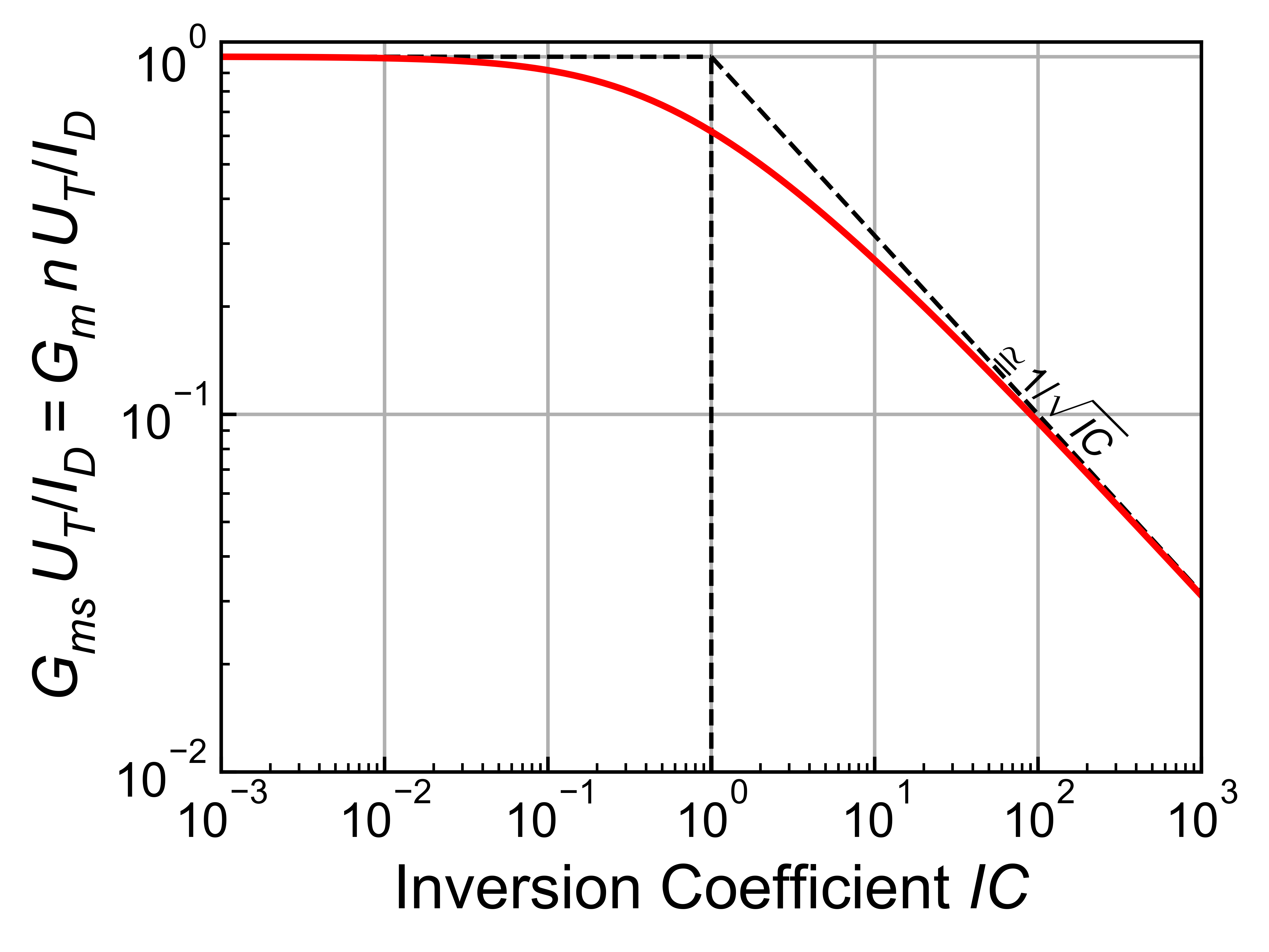
The normalized \(G_m/I_D\) ratio given by \(\eqref{eqn:4:gmsid_long}\) is plotted versus the inversion coefficient in Figure 25 in a log-log scale to highlight the asymtotic behavior. The dashed lines represent the two asymptotes of weak and strong inversion which cross at \(IC=1\). This actually led to the choice of the normalization current \(I_{spec}\) so that these two asymptotes cross at \(IC=1\). Figure 26 shows the same normalized \(G_m/I_D\) ratio versus \(IC\) but with a linear y-scale. The values of the particular points shown in Figure 26 are summarized in Table 4.
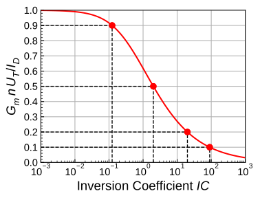
| \(IC\) | \(G_{{ms}}\,U_T/I_D = G_m\,n\,U_T/I_D\) |
|---|---|
| 0.123 | 0.9 |
| 1 | 0.618 |
| 2 | 0.5 |
| 20 | 0.2 |
| 90 | 0.1 |
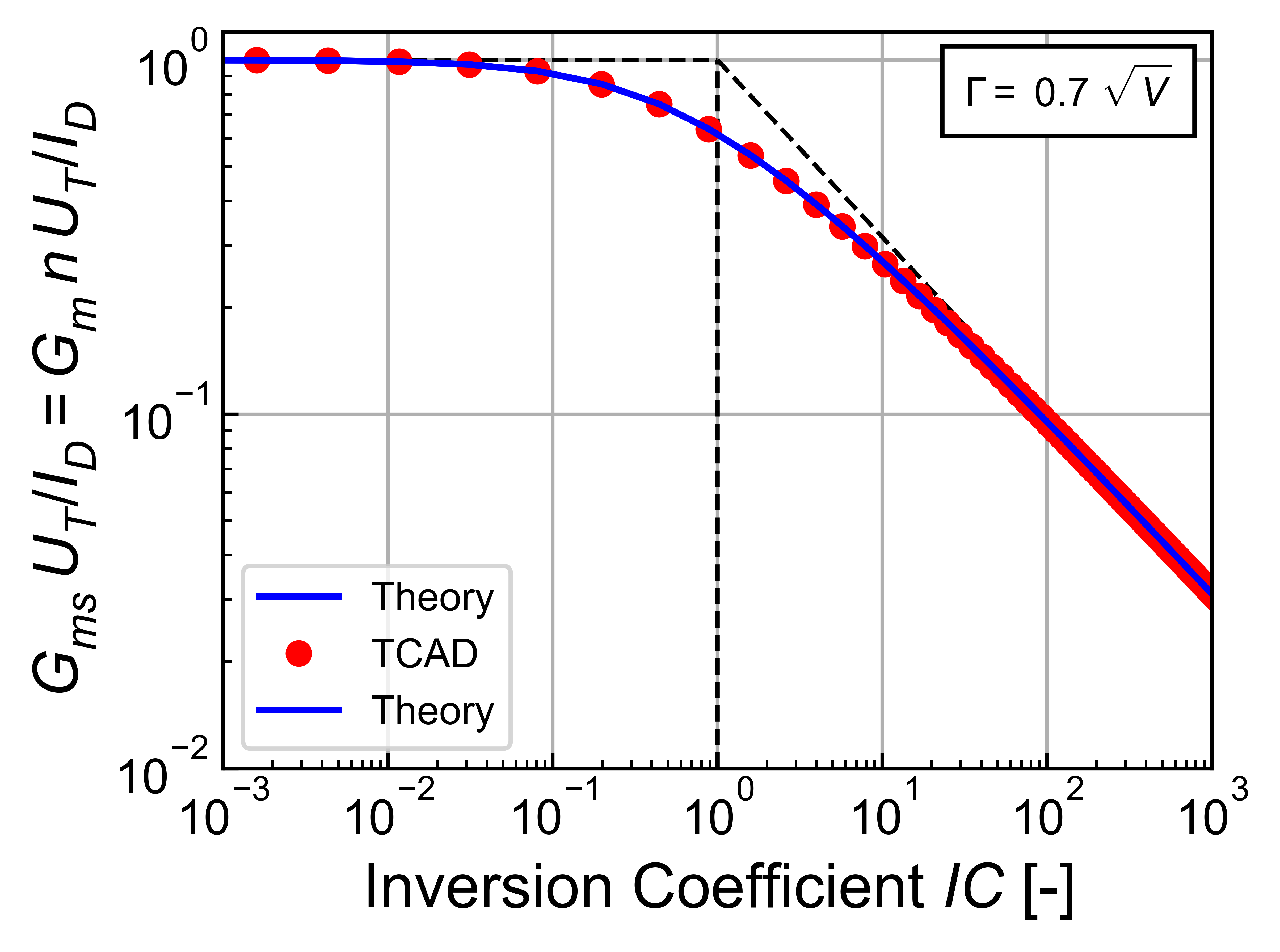
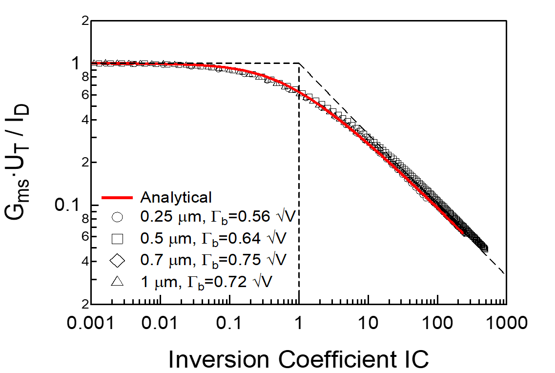
The \(G_m/I_D\) ratio has been verified with a TCAD simulation assuming \(\Gamma_b=0.7\;\sqrt{V}\). The result is shown in Figure 27, which shows an almost perfect match. Figure 28 shows the normalized \(G_m/I_D\) ratio measured on various old CMOS technologies. We see that, after proper normalization, all the measurements points fall on the analytical expression. This shows how the normalization process can strip away the dependence to a particular technology. It also illustrates the invariance of the normalized \(G_m/I_D\) ratio to CMOS technology scaling (assuming long-channel devices).
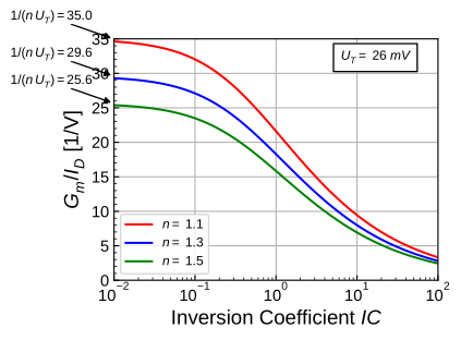
The \(G_m/I_D\) is often used as the main design parameter instead of the inversion coefficient \(IC\) [21] [22]. It is plotted in Figure 29 for different values of the slope factor \(n\) at room temperature. We see that the weak inversion asymptote \(1/(n\,U_T)\) depends on \(n\) and on temperature and typically ranges from 25 to 35 \(V^{-1}\). Although equivalent, the drawback of using the \(G_m/I_D\) ratio instead of \(IC\) is that \(G_m/I_D\) depends on \(n\,U_T\) and therefore on a given technology. This is not the case of \(IC\). Another drawback is the saturation of the \(G_m/I_D\) when reaching weak inversion, which may result in a large error on the inversion coefficient when imposing \(G_m/I_D\).
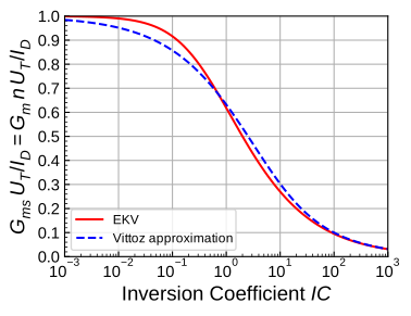
We can also use the interpolation function by Cerveny and Vittoz [19], [15] and given in \(\eqref{eqn:4:if_vps_vittoz}\). This leads to \[\begin{equation}\label{eqn:4:gmid_vittoz} \frac{G_{ms} \cdot U_T}{I_D} = \frac{G_m \cdot n\,U_T}{I_D} = \frac{1-e^{-\sqrt{IC}}}{\sqrt{IC}}. \end{equation}\]
The normalized \(G_m/I_D\) function given by \(\eqref{eqn:4:gmid_vittoz}\) is compared to the EKV expression given by \(\eqref{eqn:4:gmsid_long}\) in Figure 30. We see that the approximation \(\eqref{eqn:4:gmid_vittoz}\) slightly underestimates the \(G_m/I_D\) below \(IC=1\) and overestimates it for \(IC\) between 1 and 100.
4.3.2 The High-frequency Small-signal Model
4.3.2.1 Intrinsic High-frequency Model
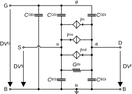
The small-signal circuit of Figure 20 is only valid at low-frequency. To extend it to high-frequency we need to add the five intrinsic capacitances \(C_{GSi}\), \(C_{GDi}\), \(C_{GBi}\), \(C_{BSi}\) and \(C_{BDi}\) as shown in Figure 31. We also need to add three transcapacitances \(C_m\), \(C_{ms}\) and \(C_{md}\) that can be embedded into the VCCS that are used for the transconductances. The VCCS currents \(I_m\), \(I_{ms}\) and \(I_{md}\) are then given by \[\begin{align} I_m &= Y_m(s) \cdot \Delta V_G,\\ I_{ms} &= Y_{ms}(s) \cdot \Delta V_S,\\ I_{md} &= Y_{md}(s) \cdot \Delta V_D, \end{align}\] where \[\begin{align} Y_m &= G_m - j\omega \cdot C_m,\\ Y_{ms} &= G_{ms} - j\omega \cdot C_{ms},\\ Y_{md} &= G_{md} - j\omega \cdot C_{md}. \end{align}\]
Note
A transcapacitance is similar to a transconductane. It is modelled by a VCCS that is controlled by the time derivative of the control voltage instead of the control voltage itself like it is the case for transcondcutances. A capacitance is controlled by the time derivative of the voltage across it.
These capacitances and transcapacitances model the charging currents at the four terminals that are needed to change the charges in the channel, in the depletion capacitance and on the gate. They are obviously bias dependent. The derivation of all these capacitances and transcapacitantes is tedious and will not be detailed here. It is done in the specialized notebook “Intrinsic Capacitances”. All these capacitances and transcapacitances are actually proportional to the total gate capacitance \(C_{OX} \triangleq W\,L\,C_{ox}\). Their bias dependence is captured by the capacitances and transcapacitances normalized to \(C_{OX}\). It can be shown that we only need to compute three normalized capacitances. They are expressed in terms of \(n\), \(q_s\) and \(q_d\). Three others can be computed by using the source-drain symmetry by swapping \(q_s\) and \(q_d\) in the expressions. The remaining capacitances can be computed by using some basic relations among them derived from the charge conservation and depletion charge relations. This leads to the following expressions \[\begin{align} c_{gsi} &\triangleq \frac{C_{GSi}}{C_{OX}} = \frac{q_s}{3} \cdot \frac{2 q_s + 4 q_d + 3}{(q_s + q_d + 1)^2},\\ c_{gdi} &\triangleq \frac{C_{GDi}}{C_{OX}} = \frac{q_d}{3} \cdot \frac{2 q_d + 4 q_s + 3}{(q_s + q_d + 1)^2},\\ c_{gbi} &\triangleq \frac{C_{GBi}}{C_{OX}} = \frac{n-1}{n} \cdot (1-c_{gsi}-c_{gdi}) = \frac{n-1}{3 n} \cdot \frac{q_s^2 + q_d^2 - 2 q_s q_d + 3 q_s + 3 q_d + 3}{(q_s + q_d + 1)^2},\\ c_{bsi} &\triangleq \frac{C_{BSi}}{C_{OX}} = (n-1) \cdot c_{gsi},\\ c_{bdi} &\triangleq \frac{C_{BDi}}{C_{OX}} = (n-1) \cdot c_{gdi}. \end{align}\]
The five intrinsic capacitances normalized to \(C_{OX} = W \cdot L \cdot C_{ox}\) are plotted versus the normalized pinch-off voltage \(v_p\) in Figure 32 and versus the normalized drain voltage in Figure 33.
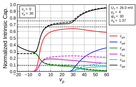
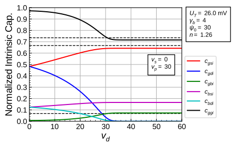
We see that in strong inversion and saturation they are approximately given by \[\begin{align} c_{gsi} &\cong \frac{2}{3},\\ c_{gdi} &\cong 0,\\ c_{gbi} &\cong \frac{n-1}{3 n},\\ c_{bsi} &\cong (n-1) \cdot \frac{2}{3},\\ c_{bdi} &\cong 0. \end{align}\] Note that the dashed curves in Figure 32 are calculated with a constant slope factor \(n_0\) calculated for \(v_p=0\).
It can be shown that the transadmitances \(Y_m\), \(Y_{ms}\) and \(Y_{md}\) can be written as \[\begin{align} Y_m &= G_m \cdot (1 - j\omega \cdot \tau_{qs}),\\ Y_{ms} &= G_{ms} \cdot (1 - j\omega \cdot \tau_{qs}),\\ Y_{md} &= G_{md} \cdot (1 - j\omega \cdot \tau_{qs}). \end{align}\] where \(\tau_{qs} = C_m/G_m = C_{ms}/G_{ms} = C_{md}/G_{md}\) is the quasi-static time constant related to the propagation time along the channel which depends on \(q_s\) and \(q_d\) according to \[\begin{equation}\label{eqn:4:tauqs} \frac{\tau_{qs}}{\tau_{spec}} = \frac{1}{30}\,\frac{4 q_s^2 + 4 q_d^2 + 12 q_s q_d + 10 q_s + 10 q_d + 5}{(q_s + q_d + 1)^3}, \end{equation}\] with \(\tau_{spec}\) defined as \[\begin{equation} \tau_{spec} = \frac{1}{\omega_{spec}} \triangleq \frac{L^2}{\mu \cdot U_T}. \end{equation}\]
Note
Notice that \(\tau_{spec}\) and therefore \(\tau_{qs}\) scale with the square of the length \(L\) and therefore take full advantage of technology down-scaling.
Note
Notice the symmetry of the model in \(\eqref{eqn:4:tauqs}\). Indeed, swapping \(q_s\) and \(q_d\) does not change \(\eqref{eqn:4:tauqs}\).
The frequency \(\omega_{qs} \triangleq 1/\tau_{qs}\) corresponds to the limit of validity of the quasi-static (QS) model. The lumped model shown in Figure 31 does not hold anymore above \(\omega_{qs}\) and a non-quasi-static (NQS) model is required to account for the distributed nature of the channel [23].
The normalized QS frequency \(\Omega_{qs}\) is given by \[\begin{equation}\label{eqn:4:Omegaqs_qs_qd} \Omega_{qs} \triangleq \frac{\omega_{qs}}{\omega_{spec}} \triangleq \frac{\tau_{spec}}{\tau_{qs}} = 30 \cdot \frac{(q_s + q_d + 1)^3}{4 q_s^2 + 4 q_d^2 + 12 q_s q_d + 10 q_s + 10 q_d + 5}. \end{equation}\] In saturation, \(\eqref{eqn:4:Omegaqs_qs_qd}\) reduces to \[\begin{equation}\label{eqn:4:Omegaqs_qs_sat} \Omega_{qs} \cong 30 \cdot \frac{(q_s + 1)^3}{4 q_s^2 + 10 q_s + 5} = \begin{cases} 6 & \textsf{in WI and sat.,}\\ \frac{15}{2} \cdot q_s = \frac{15}{2} \cdot \sqrt{IC} \cong \frac{15}{4} \cdot \frac{V_P-V_S}{U_T}& \textsf{in SI and sat.} \end{cases} \end{equation}\] From \(\eqref{eqn:4:Omegaqs_qs_qd}\), we see that in weak inversion \(\omega_{qs} = 6\,\omega_{spec} = 6\,\mu \cdot U_T/L^2\) which is bias-independent and only determined by the mobility and the transistor length. Note that in weak inversion, \(\tau_{qs} = 1/\omega_{qs}\) corresponds to the transit time of the carriers diffusing from source to drain, similarly to the transit time of carrier through the base of a bipolar transistor. In strong inversion, \(\Omega_{qs}\) is proportional to \(q_s\) or to \(\sqrt{IC}\) or to the saturation voltage \(V_{DSsat} = V_P-V_S\).
The transcapacitances can then be expressed as \[\begin{align} C_m &= G_m \cdot \tau_{qs},\\ C_{ms} &= G_{ms} \cdot \tau_{qs},\\ C_{md} &= G_{md} \cdot \tau_{qs}. \end{align}\]
The three transcapacitances normalized to \(C_{OX} = W \cdot L \cdot C_{ox}\) are plotted versus the normalized pinch-off voltage \(v_p\) in Figure 34 and versus the normalized drain voltage \(v_d\) in Figure 35.
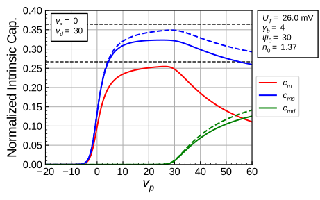
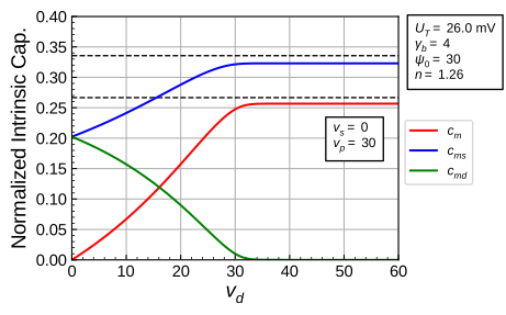
We see that the normalized transcapacitances in strong inversion and saturation are approximately given by \[\begin{align} c_m &\cong \frac{4}{15},\\ c_{ms} &\cong n \cdot \frac{4}{15},\\ c_{md} &\cong 0. \end{align}\]
In the same way there is a relation between the gate transconductance and the source and drain transconductances, the gate transadmittance is given by \[\begin{equation}\label{eqn:4:Ym_Yms_Ymd} Y_m = \frac{Y_{ms} - Y_{md}}{n}. \end{equation}\] From \(\eqref{eqn:4:Ym_Yms_Ymd}\), we also have \[\begin{equation} C_m = \frac{C_{ms} - C_{md}}{n}. \end{equation}\]
The intrinsic capacitances \(c_{gsi}\), \(c_{gbi}\), \(c_{bsi}\) and the transcapacitances \(c_m\) and \(c_{ms}\) in saturation (i.e. for \(q_d=0\)) are plotted versus \(IC\) in Figure 36.
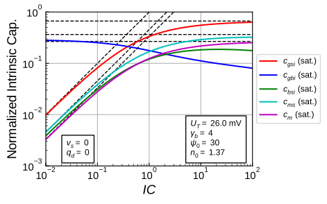
We see that the intrinsic capacitances basically become negligible in wmoderate and weak inversion, except \(c_{gbi}\). The transistor parasitic capacitances in moderate and weak inversion are therefore dominated by the extrinsic capacitances which are presented in the next section.
4.3.3 Extrinsic capacitances
In addition to the intrinsic capacitances, we also need to add the extrinsic capacitances. The latter include the overlap, fringing field and junction capacitances.
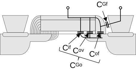
The overlap and fringing field capacitances are illustrated in Figure 37. The overlap capacitances are due to the electric field between the gate and the channel \(C_{if}\), the source and drain extensions through the oxyde \(C_{ov}\) and through the spacer \(C_{of}\). Although these capacitances show some bias dependence, they are modelled by two bias-independent capacitances, \(C_{GSo}\) between the gate and the source and \(C_{GDo}\) between the gate and the drain. They scale with the transistor width \(W\) so that \(C_{GSo} = W \cdot C_{Go}\) and \(C_{GDo} = W \cdot C_{Go}\) but are independent of the transistor length. Their value is therefore specified by a capacitance per transistor width \(C_{Go}\) which is usually equal on the source and drain sides so that \[\begin{align} C_{GSo} &= W \cdot C_{Go},\\ C_{GDo} &= W \cdot C_{Go}. \end{align}\]
In advanced technologies, the gate stack is close to the source or drain vias, introducing a capacitive coupling between the gate and the source and between the gate and the drain. They are also modeled by two bias-independent capacitances \(C_{GSf}\) and \(C_{GDf}\) which also scale with the width of the transistor and are symmetrical with respect to source and drain so that \[\begin{align} C_{GSf} &= W \cdot C_{Gf},\\ C_{GDf} &= W \cdot C_{Gf}. \end{align}\]
All the overlap and fringing field capacitances can be added into two extrinsic capacitances, \(C_{GSe} = C_{GSo} + C_{GSf}\) between the gate and the source and \(C_{GDe} = C_{GDo} + C_{GDf}\) between the gate and the drain. Since they all scale with \(W\), we can write \[\begin{align} C_{GSe} &= W \cdot C_{Ge},\\ C_{GDe} &= W \cdot C_{Ge}, \end{align}\] with \[\begin{equation}\label{eqn:4:} C_{Ge} = C_{Go} + C_{Gf}. \end{equation}\]
The gate-to-source extrinsic capacitances \(C_{GSe}\) comes in parallel to the gate-to-source intrinsic capacitance \(C_{GSi}\) and can therfore be added to \(C_{GSi}\). Similalry at the drain, \(C_{GDe}\) can be added to \(C_{GDi}\).
There is also an overlap capacitance between the gate and the bulk which is usually much smaller than the overlap capacitances between the gate and the source and the gate and the drain.
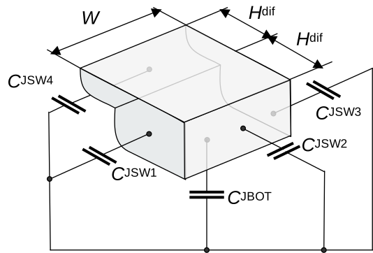
In addition to the overlap and fringing field capacitances, we also have to account for the junction capacitances at the source and drain. As illustrated in Figure 38, the junction capacitances are splitted into a bottom junction capacitance \(C_{JBOT}\), outer side-wall capacitances on the STI side \(C_{JSW1}\), \(C_{JSW2}\) and \(C_{JSW3}\) and an inner side-wall capacitance on the gate side \(C_{JSW4}\). The total junction capacitance between the drain (source and the bulk (or the well) are given by \[\begin{equation} C_{J,tot} = C_{JBOT} + C_{JSW,out} + C_{JSW,in} \end{equation}\] with \[\begin{align} C_{JBOT} &= CJ \cdot W \cdot 2 H_{dif},\\ C_{JSW,out} &= CJSW \cdot (W + 2 H_{dif}),\\ C_{JSW,in} &= CJSWG \cdot W. \end{align}\] All the above junction capacitances are bias-dependent. However, in the design phase, we can estimate them for zero bias voltage value which is a worst case value. Parameters \(CJ\), \(CJSW\) and \(CJSWG\) are technology parameters corresponding to the zero-bias values.
For design optimization, it is useful to split the total junction capacitance into a constant part \(C_{J0}\) and a part that scales with \(W\) \[\begin{equation} C_{J,tot} = C_{J0} + C_{JW} \cdot W \end{equation}\] with \[\begin{align} C_{J0} &= CJSW \cdot 2 H_{dif},\\ C_{JW} &= CJSW + CJSWG + CJ \cdot 2 H_{dif}. \end{align}\]
4.3.3.1 Full High-frequency Model
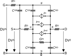
The intrinsic small-signal schematic of Figure 31 needs to be completed by the components related to the extrinsic part of the transistor as shown in Figure 39. This includes the access resistances \(R_S\), \(R_D\) and \(R_G\) and the five extrinsic capacitances \(C_{GSe}\), \(C_{GDe}\), \(C_{GBe}\), \(C_{BSj}\) and \(C_{BDj}\) which come in parallel to the five intrinsic capacitances \[\begin{align} &C_{GS} = C_{GSi} + C_{GSe},\\ &C_{GD} = C_{GDi} + C_{GDe},\\ &C_{GB} = C_{GBi} + C_{GBe},\\ &C_{BS} = C_{BSi} + C_{BSj},\\ &C_{BD} = C_{BDi} + C_{BDj}. \end{align}\] \(C_{GSe}\), \(C_{GDe}\) and \(C_{GBe}\) include the overlap and fringing field capacitances, whereas \(C_{BSj}\) and \(C_{BDj}\) are the junction capacitances of the source and drain diffusions.
For low-power applications it is essential to also consider the noise which is generated in the device and which constitutes the lower limit of resolution. The small-signal schematic will be completed with the noise sources in the next section.
4.4 The noise model
In any circuit noise analysis problem, there are always two aspects to deal with: the first is to identify and characterize all the various noise sources coming from the noisy devices and second to evaluate how all these noise sources propagate to the output of the circuit. In this section we characterize and model the noise generated in the MOS transistor.
For long-channel tansistors, there are mainly two kinds of noise in the MOS transistor: thermal and flicker noise. We start looking at the thermal noise first.
4.4.1 Thermal noise
4.4.1.1 Thermal noise conductance
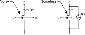
If we assume that the transistor is biased in the linear region with \(V_D=V_S\), the channel is then uniform and the transistor behaves like a resistor. It therefore seems obvious that this resistive channel will produce thermal noise generating drain current fluctuations that can be modelled as shown in Figure 40 by a noisy current source connected between the drain and the source and having a PSD [15] \[\begin{equation}\label{eqn:4:sind} S_{\Delta I_{nD}^2} = 4 k_B T \cdot G_n, \end{equation}\] where \(G_n\) is the thermal noise conductance at the drain which in this case is simply equal to the channel conductance \(G_{dso} = G_{ms}\). In the case \(V_D\) is larger than \(V_S\), the channel is no more uniform but the drain current fluctuations due to thermal noise can still be written as \(\eqref{eqn:4:sind}\) with the noise conductance given by [15] \[\begin{equation} G_n = \frac{\mu}{L^2} \cdot |Q_I|, \end{equation}\] where \(Q_I\) is the total mobile (or inversion) charge stored in the channel. Of course the thermal noise conductance \(G_n\) depends on bias. It can be shown that the normalized thermal noise conductance \(g_n\) depends on \(q_s\) and \(q_d\) according to [15] \[\begin{equation}\label{eqn:4:gn_qs_qd} g_n \triangleq \frac{G_n}{G_{spec}} = \frac{1}{6} \cdot \frac{4q_s^2+3q_s+4q_sq_d+3q_d+4q_d^2}{q_s+q_d+1}. \end{equation}\] Equation \(\eqref{eqn:4:gn_qs_qd}\) illustrates once more the symmetry of the model. Indeed, the expression of \(g_n\) remains unchanged when swapping \(q_s\) and \(q_d\).
It is interesting to first evaluate \(\eqref{eqn:4:gn_qs_qd}\) in the linear region by setting \(q_s=q_d\) resulting in \[\begin{equation} g_n = q_s = g_{ms}, \end{equation}\] or in denormalized form \[\begin{equation} G_n = G_{spec} \cdot q_s = G_{ms}. \end{equation}\] This shows that the thermal noise conductance at the drain is simply equal to the source transconductance which in the linear region is equal to the channel conductance. This is consistent with the observation made above.
In saturation \(q_s \gg q_d\) and \(\eqref{eqn:4:gn_qs_qd}\) simplifies to \[\begin{equation}\label{eqn:4:gn_sat} g_n = \tfrac{2}{3}\,q_s \cdot \frac{q_s+\tfrac{3}{4}}{q_s+1} \quad \textsf{in saturation}, \end{equation}\] which in strong inversion, \(q_s \gg 1\) becomes \[\begin{equation} g_n = \tfrac{2}{3}\,q_s = \tfrac{2}{3}\,g_{ms} \end{equation}\] or in denormalized form \[\begin{equation} G_n = \tfrac{2}{3}\,G_{ms} = \tfrac{2}{3} n\,G_m. \end{equation}\] The thermal noise conductance in strong inversion and saturation is proportional to \(G_{ms}\) (or \(G_m\)) but with a proportionality factor \(\tfrac{2}{3}\) (\(\tfrac{2}{3} n\) when writing in terms of \(G_m\)) instead of one. This is due to the channel being non-uniform between the source and the drain and pinched-off at the drain, resulting in less noise than what a uniform channel with the same conductance \(G_{ms}\) would produce.
In weak inversion, \(q_s \ll 1\) and \(q_d \ll 1\), and \(\eqref{eqn:4:gn_qs_qd}\) simplifies to \[\begin{equation} g_n \cong \frac{q_s+q_d}{2}. \end{equation}\] Now in weak inversion, \(q_s=i_f\) and \(q_d=i_r\) and hence \[\begin{equation} g_n \cong \frac{i_f+i_r}{2}. \end{equation}\] The denormalized thermal noise conductance then writes \[\begin{equation} G_n = G_{spec} \cdot g_n = \frac{I_{spec}}{U_T} \frac{i_f+i_r}{2} = \frac{I_F+I_R}{2U_T}. \end{equation}\] The PSD is then given by \[\begin{equation} S_{\Delta I_{nD}^2} = 4 k_B T \cdot G_n = 4 k_B T \cdot \frac{I_F+I_R}{2U_T} = 2q \, (I_F+I_R). \end{equation}\]
This shows that, even though the noise PSD has been derived assuming that the local noise current source is thermal noise, the PSD in weak inversion actually corresponds to full shot noise of both the forward and the reverse components. This result is consistent with the fact that the drain current in weak inversion is dominated by the diffusion current controlled by the potential barriers at the source (controlling \(I_F\)) and at the drain (controlling \(I_R\)).
4.4.1.2 Thermal noise factors
Several thermal noise factors can be defined according to the definitions introduced initially by van der Ziel [24]. The thermal noise parameter related to the drain terminal \(\delta_n\) is defined as [15] [25] [26] \[\begin{equation}\label{eqn:4:deltand_def} \delta_n \triangleq \frac{G_n}{G_{dso}}, \end{equation}\] where \(G_{dso}\) is the drain-to-source conductance at \(V_{DS} = 0\), \[\begin{equation}\label{eqn:4:gdo} G_{dso} = G_{ms} = G_{spec} \cdot q_s. \end{equation}\]
Note
Van der Ziel initially used \(\gamma\) for the thermal noise parameter defined by \(\eqref{eqn:4:deltand_def}\) and \(\alpha\) for the noise excess factor defined by \(\eqref{eqn:4:gammand_def}\). The most important noise excess factor from a circuit design point of view is the one given by \(\eqref{eqn:4:gammand_def}\), which has been called \(\gamma\) in many papers instead of \(\alpha\) as it was defined initially by Van der Ziel [24]. We will keep the circuit design definition of \(\gamma\) and rename the Van der Ziel’s \(\gamma\) as \(\delta\).
The \(\delta_n\) parameter shows how much the thermal noise of the active device deviates from the value it takes when it operates as a passive resistor of conductance \(G_{dso}\). Since for \(V_{DS} = 0\) the noise conductance \(G_n\) is equal to the channel conductance \(G_{dso}\), the noise parameter \(\delta_n\) is then equal to unity.
Assuming constant mobility, it can be shown that \(\delta_n\) can be written in terms of the normalized charges as \[\begin{equation} \delta_n = \frac{g_n}{g_{ms}} = \frac{g_n}{q_s} = \tfrac{1}{6} \cdot \frac{4q_s^2+3q_s+4q_sq_d+3q_d+4q_d^2}{q_s\,(q_s+q_d+1)}. \end{equation}\]
In saturation (i.e. for \(q_d=0\)), \(\delta_n\) simplifies to \[\begin{equation}\label{eqn:4:deltansat} \delta_n = \tfrac{2}{3} \cdot \frac{q_s + \tfrac{3}{4}}{q_s + 1} = \begin{cases} \frac{1}{2} & \textsf{WI and saturation ($q_s \ll 1$),}\\ \frac{2}{3} & \textsf{SI and saturation ($q_s \gg 1$).} \end{cases} \end{equation}\]
Note that the \(\delta_n\) thermal noise parameter compares the thermal noise conductance evaluated at a given operating point that is not necessarily the same as the one used to define the output conductance \(G_{dso}\) (i.e. \(V_{DS} = 0\)). It is therefore not very useful for circuit design and is used more for modeling purposes.
For circuit design, it is more useful to define another figure-of-merit (FoM) \(\gamma_n\), named the thermal noise excess factor related to the drain and defined as \[\begin{equation}\label{eqn:4:gammand_def} \gamma_n \triangleq \frac{G_n}{G_m} = \frac{g_n}{g_m}. \end{equation}\] Contrary to the \(\delta_n\) thermal noise parameter, the noise conductance \(G_n\) and the gate transconductance \(G_m\) used in the definition \(\eqref{eqn:4:gammand_def}\) are evaluated at the same operating point.
Important
The \(\gamma_n\) FoM represents how much noise is generated at the drain of a transistor for a given gate transconductance.
We will see that \(\gamma_n\) has a direct impact on the noise performance of circuits, particularly at RF where the noise is dominated by thermal noise [27]. The smaller \(\gamma_n\), the better the noise performance of the device. Note that \(\gamma_n\) can become quite large in the linear region when \(V_D\) tends to \(V_S\). Indeed, in this region, the gate transconductance gets smaller as the drain-to-source voltage decreases, but the thermal noise conductance does not decrease, resulting in a degradation of the \(\gamma_n\) noise excess factor. At the limit when \(V_D\) becomes equal to \(V_S\), the gate transconductance becomes zero and \(\gamma_n\) tends to infinity. This is why the thermal noise excess factor is mostly used for a transistor biased in saturation.
Note
Note that \(\gamma_n\) is also a FoM that can be used for any transconductor (even for circuit transconductors like OTAs) to evaluate how much thermal noise is generated for a given transconductance. The smaller \(\gamma_n\), the better the transconductor.
The thermal noise excess factor \(\gamma_n\) is obviously related to the thermal noise parameter \(\delta_n\) by \[\begin{equation}\label{eqn:4:gammand_deltand} \gamma_n = \frac{G_n}{G_{dso}} \cdot \frac{G_{dso}}{G_m} = \delta_n \cdot \frac{G_{dso}}{G_m} = \delta_n \cdot n \cdot \frac{G_{ms}}{G_{ms} - G_{md}}. \end{equation}\] In saturation, \(G_{md} = 0\), resulting in \[\begin{equation}\label{eqn:4:6:gammandsat_def} \gamma_n = \delta_n \cdot n = \begin{cases} \frac{n}{2} & \textsf{WI and saturation,} \\%[3mm] \frac{2}{3} \cdot n & \textsf{SI and saturation,} \end{cases} \end{equation}\] since \(G_{dso} = G_{ms}\). For \(n=1.5\), the thermal noise excess factor in strong inversion and saturation is approximately equal to unity and the thermal noise conductance is about equal to the gate transconductance \(G_n \cong G_m\).
The PSD of the drain current thermal noise fluctuations can then be written in terms of the noise excess factors and the transconductances as \[\begin{equation}\label{eqn:4:Snth} S_{\Delta I_{nD}^2} = 4 k_B T \cdot \delta_n \cdot G_{ms} = 4 k_B T \cdot \gamma_n \cdot G_m, \end{equation}\]
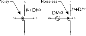
As shown in Figure 41, the drain current noise can be referred to the gate by dividing the drain PSD \(S_{\Delta I_{nD}^2}\) by the square of the gate transconductance \(G_m\) \[\begin{equation} S_{\Delta V_{nG}^2} = \frac{S_{\Delta I_{nD}^2}}{G_m^2} = 4 k_B T \cdot R_n, \end{equation}\] where \(R_n\) is the input-referred (or gate-referred) thermal noise resistance given by \[\begin{equation}\label{eqn:4:input_referred_thermal_noise} R_n = \frac{G_n}{G_m^2} = \frac{\gamma_n}{G_m} = \begin{cases} \tfrac{1}{2} \frac{n}{G_m} & \textsf{WI and saturation,}\\%[3mm] \tfrac{2}{3} \frac{n}{G_m} \cong \frac{1}{G_m} & \textsf{SI and saturation.} \end{cases} \end{equation}\]
From \(\eqref{eqn:4:input_referred_thermal_noise}\), we observe that the input-referred thermal noise can be decreased by increasing the transconductance, which leads to an increased current consumption.
The above relations have been derived assuming a long-channel transistor. The thermal noise of short-channel transistors actually degrades compared to long-channel devices. The thermal noise excess factor \(\gamma_n\) increases to values that can reach 3. This increase of \(\gamma_n\) can be compensated by increasing the transconductance to keep a constant input-referred noise resistance, but at the cost of higher power consumption.
4.4.1.3 The Fano noise suppression factor
The Fano noise suppression factor \(F_a\) is another way to characterize the transistor white noise initially introduced by Ugo Fano in 1947 [28], [29], [30]. \(F_a\) is usually comprised between zero and one. It has been proposed as an alternative for characterizing and modeling the white noise of devices from advanced technologies [31], [32], [33]. Another motivation to use \(F_a\) instead of \(\gamma_n\) is its small dependence on temperature which is an interesting feature to model the noise down to cryogenic temperature [34].
In this Section we will show that the Fano noise suppression factor is actually proportional to \(G_m/I_D\) and can therefore be expressed in terms of the inversion coefficient \(IC\) [8], [9].
The thermal noise excess factor \(\gamma_n\) introduced above compares the effective PSD of the drain current fluctuations to the thermal noise of a conductance of value \(G_m\). Another approach is to compare the PSD of the drain current fluctuations to the PSD of shot noise which is dominant in weak inversion. This definition corresponds to the Fano noise suppression factor \(F_a\). By definition \(F_a=1\) when the noise is full shot noise like in WI and \(F_a<1\) when the noise is only partially due to shot noise like it is the case in moderate and strong inversion for example. We can derive the expression of \(F_a\) by equating \(\eqref{eqn:4:Snth}\) to \[\begin{equation} S_{\Delta I_{nD}^2} = F_a \cdot 2 q I_D, \end{equation}\] and solving for \(F_a\) which results in [35] \[\begin{equation}\label{eqn:4:fano_def} F_a = \frac{S_{\Delta I_{nD}^2}}{2 q I_D} = 2 \gamma_n \cdot U_T \cdot \frac{G_m}{I_D}, \end{equation}\] which can also be written in terms of \(IC\) as [35] \[\begin{equation}\label{eqn:4:fano_ic} F_a(IC) = 2 \frac{\gamma_n(IC)}{n} \cdot \frac{g_{ms}(IC)}{IC} = 2 \delta_n(IC) \cdot \frac{g_{ms}(IC)}{IC}. \end{equation}\] Equation \(\eqref{eqn:4:fano_ic}\) shows that \(F_a\) is actually proportional to the normalized \(G_m/I_D\) FoM given by \(\eqref{eqn:4:gmsid_long}\) and the proportionality factor is two times \(\delta_n\) [35]. For a long-channel transistor in saturation, the bias dependence of \(\delta_n\) remains small since it varies from \(1/2\) to \(2/3\). This means that the bias dependence of \(F_a\) is mostly captured by the \(G_m/I_D\) ratio which is often used as a FoM for low-power design since it gives the transconductance that can be achieved for a given drain current in saturation at a given \(IC\). Since \(G_m/I_D\) is maximum in weak inversion, optimizing the \(G_m/I_D\) FoM is done by setting the bias as much in WI as other specifications allow (namely speed or gain-bandwidth product). This results in the maximum \(F_a\), meaning a maximum of white noise PSD for a given current. This perfectly illustrates the trade-off between power consumption and noise.
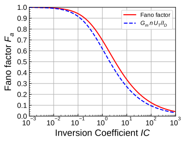
Combining \(\eqref{eqn:4:fano_ic}\), \(\eqref{eqn:4:gmsid_long}\) and \(\eqref{eqn:4:deltansat}\), the Fano noise suppression factor only depends on the inversion coefficient. It is plotted versus \(IC\) in Figure 42 and compared to the normalized \(G_m/I_D\) FoM. Figure 42 shows that \(F_a\) is actually very close to the normalized \(G_m/I_D\) function and ultimately tends to zero for large inversion coefficient. The difference is due to the dependence of \(\delta_n\) with \(IC\). Since in weak inversion \(g_{ms}/IC \cong 1\) and \(\delta_n \cong 1/2\) then \(F_a \cong 1\) as expected. In strong inversion, \(g_{ms}/IC \cong 1/\sqrt{IC}\) and \(\delta_n \cong 2/3\), \(F_a \cong 4/(3 \sqrt{IC})\).
Note that the above analysis does not account for the short-channel effects which are discussed in the short-channel model Chapter.
4.4.2 Flicker noise
In addition to the thermal noise of the channel described above, the MOS transistor also exhibits flicker or 1/f noise. As its name suggests, flicker noise is characterized by a PSD that is inversely proportional to frequency. It therefore mainly dominates at low-frequency, below the so-called corner frequency \(f_k\) defined as the frequency at which 1/f noise contributes equally than the white noise to the total noise PSD (referred indifferently at the drain or at the gate). Because the 1/f noise scales inversely proportional to the gate area, it is becoming a major issue for analog IC design in deep and ultra deep submicron devices. Corner frequencies of several tens of MHz are now typical and hence low-frequency analog circuits are usually totally dominated by 1/f noise. Techniques exist to reduce or even eliminate this low-frequency noise. The most obvious one is to size the gate area in order to bring down the corner frequency to an acceptable value. This is done at the expense of higher capacitances, which require higher transconductance and hence higher current for the same characteristic frequency. Other circuit techniques such as chopper stabilization and correlated double sampling can be used to eliminate the 1/f noise [36], [37]. They are presented in Chapter?.
Because the most important cause of flicker is trapping of mobile charges in traps located in the oxide or at the \(Si\text{-}SiO_2\) interface, it is essential to refer the noise directly to the gate as shown in Figure 43. This avoids having the strong dependence introduced by \(G_m^2\) that appears in the drain current fluctuations. The flicker noise referred to the gate can be modelled as in EKV 2.6 by a PSD given by [38] \[\begin{equation}\label{eqn:4:SVnG_flicker} S_{\Delta V_{nG}^2}(f) = \frac{K_F}{W_{eff}\,L_{eff}\,C_{ox}\,f^{AF}}, \end{equation}\] where \(K_F\) is a technology parameter and \(AF\) is the frequency exponent which is close to 1. Although \(AF\) is seldom exactly equal to one, we actually will assume that \(AF=1\). To simplify the design, we also will assume that \(K_F\) is constant, i.e. bias independent. As will be shown below, this is not exactly true, because \(K_F\) can show some bias dependence, typically varying by one order of magnitude over an inversion coefficient ranging from \(10^{-2}\) to \(10^2\).
In the same we modelled the gate-referred thermal noise, we can also model the flicker noise by an equivalent frequency dependent noise resistance \(R_{nf}(f)\) defined as \[\begin{equation} R_{nf}(f) \triangleq \frac{\rho}{W_{eff}\,L_{eff}\,f}, \end{equation}\] where \(\rho\) is a technology parameter given by [38] \[\begin{equation}\label{eqn:4:rho} \rho \triangleq \frac{K_F}{4\,k_B\,T\,C_{ox}}. \end{equation}\]
A more detailed study is presented in the notebook dedicated to the flicker noise model. It shows that there are basically three main causes to the flicker noise. The PSD of the gate-referred voltage fluctuations can be written as \[\begin{equation}\label{eqn:4:Sn_DVnG} S_{\Delta V_{nG}^2}(f) = \left.S_{\Delta V_{nG}^2}(f)\right|_{\Delta N} + \left.S_{\Delta V_{nG}^2}(f)\right|_{\Delta \mu} + \left.S_{\Delta V_{nG}^2}(f)\right|_{\Delta R}. \end{equation}\] The first term results from carrier fluctuations of the inversion charge due to trapping of the mobile charges in traps located in the oxide close to the \(Si\)-\(SiO_2\). This noise generation mechanism corresponds to the Mc Worther model discussed in [39]. The second term is due to fluctuations of the mobility and corresponds to the Hooge model [40]. Finally, the last term corresponds to fluctuations of the resistance of the source and drain access resistances [41] [41]. All these terms are inversely proportional to the effective gate area \(W_{eff}\,L_{eff}\) and to the frequency.
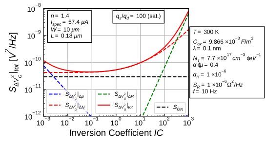
Figure 44 presents the three components of the gate-referred flicker noise PSD at \(f = 10\,Hz\) versus the inversion coefficient. The details of the model are presented in the flicker noise model notebook. Figure 44 shows that the mobility fluctuation term \(\left.S_{\Delta V_{nG}^2}(f)\right|_{\Delta \mu}\) only appears at very low \(IC\), while the access resistance contribution only contributes at very high \(IC\). In between, the gate-referred flicker noise PSD is dominated by the first term which is also bias dependent. The model presented in the notebook has been validated for a 180 nm and 90 nm bulk CMOS technologies as shown in Figure 45 and Figure 46, respectively.
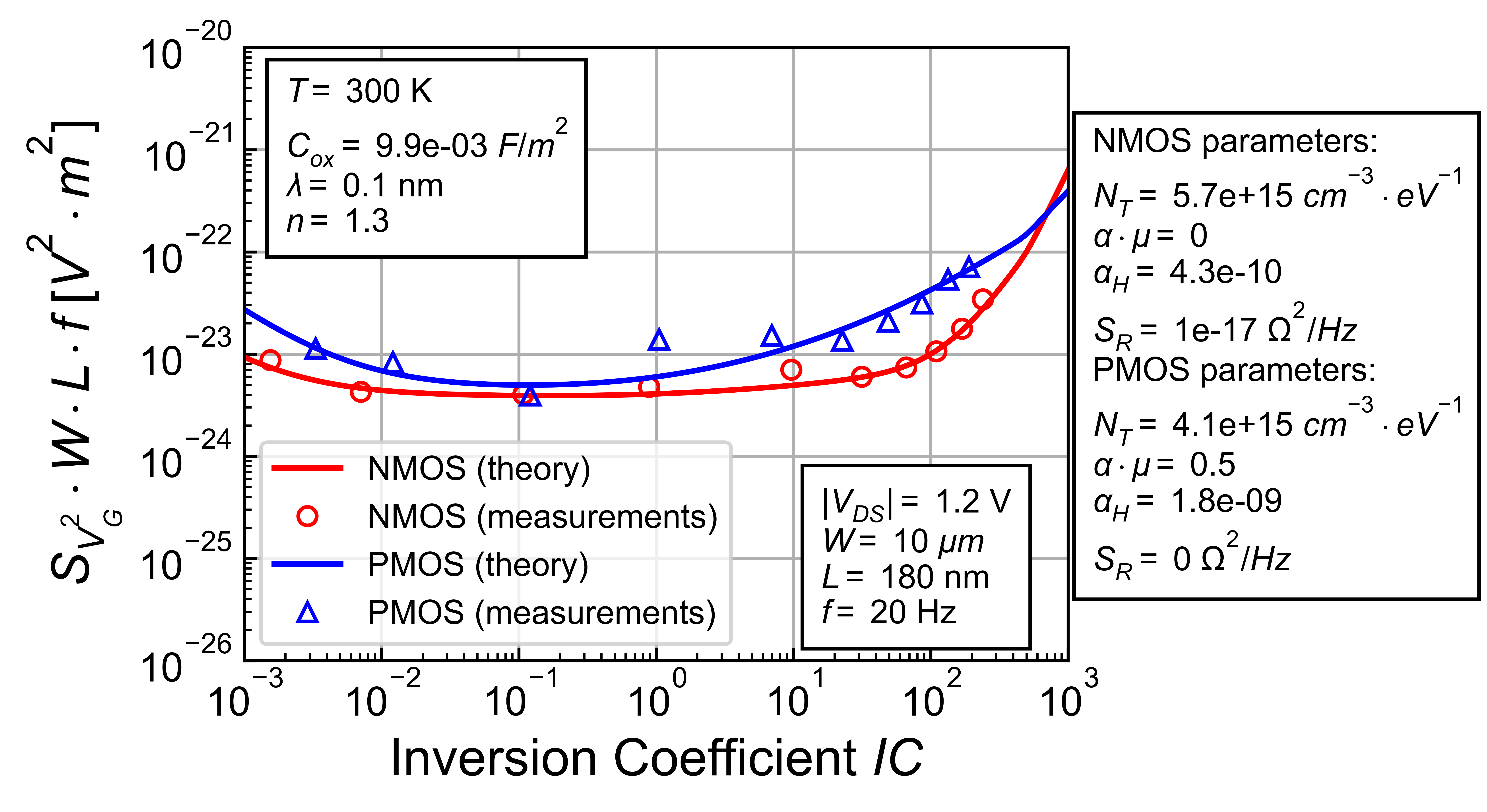
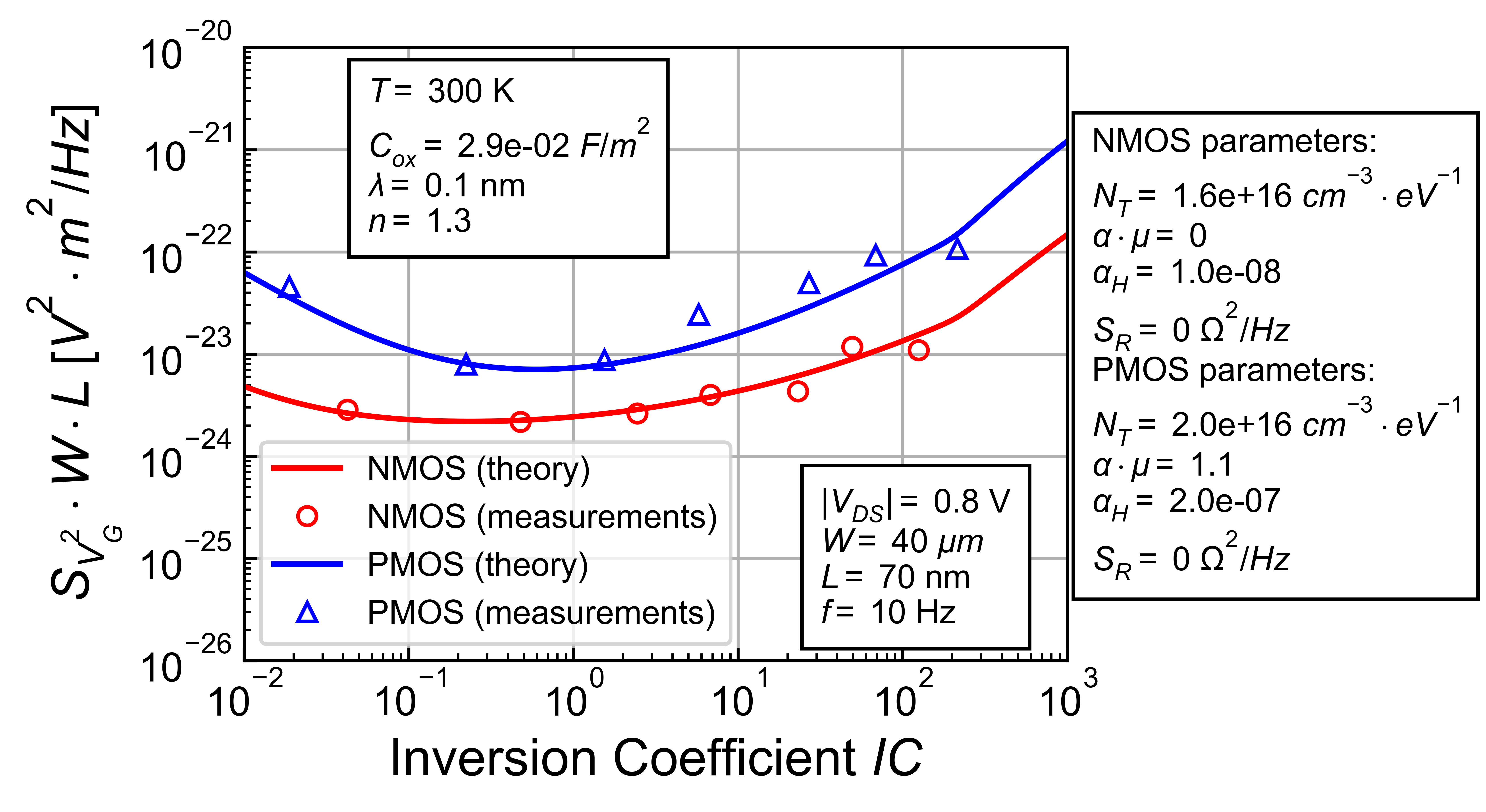
It would be cumbersome to account for the bias dependence shown in Figure 45 and Figure 46 during the design phase. For this reason we will assume that the gate-referred flicker noise is given by \(\eqref{eqn:4:SVnG_flicker}\) with \(K_F\) constant.
4.4.3 Total noise (in saturation)
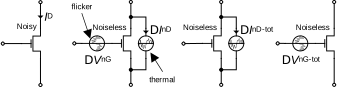
As shown in Figure 47, the noisy transistor can be represented by a noiseless transistor to which we add two noise sources: one current noise source representing the channel thermal noise and connected between the drain and the source, and one voltage noise source representing the flicker noise and connected in series with the gate. The flicker noise can be included into the noise current source between the drain and the source by multiplying it by \(G_m^2\). The PSD of the total drain current noise is then given by \[\begin{equation}\label{eqn:4:SVG_tot} S_{\Delta I_{nD,tot}^2}(f) = S_{\Delta I_{nD}^2} + G_m^2 \cdot S_{\Delta V_{nG}^2}(f) = 4 k_B T \cdot \gamma_n G_m + G_m^2 \cdot S_{\Delta V_{nG}^2}(f). \end{equation}\] Recalling that the transconductance for a given current is minimum in strong inversion, from \(\eqref{eqn:4:SVG_tot}\) we find that the noise at the drain for a given current and a given gate area is minimum in strong inversion.
It is usually more convenient to refer all the noise at the gate to compare it to the input signal voltage. The total gate noise voltage PSD is then given by \[\begin{equation} S_{\Delta V_{nG,tot}^2}(f) = \frac{S_{\Delta I_{nD,tot}^2}(f)}{G_m^2} = 4 k_B T \cdot \frac{\gamma_n}{G_m} + S_{\Delta V_{nG}^2}(f) = 4 k_B T \cdot R_{n,tot}(f), \end{equation}\] where the total gate-referred noise resistance \(R_{n,tot}(f)\) is given by \[\begin{equation} R_{n,tot}(f) = \frac{\gamma_n}{G_m} + \frac{\rho}{W \cdot L \cdot f}. \end{equation}\] Since the transconductance for a given current is maximum in weak inversion, the total gate-referred noise PSD for a given current and gate area is minimum in weak inversion.
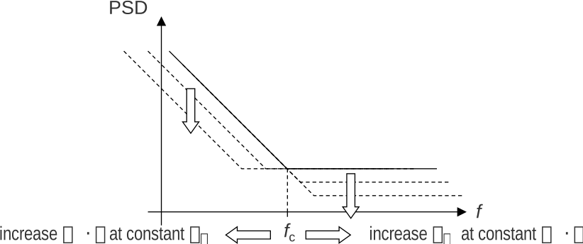
The corner frequency \(f_k\) is defined as the frequency for which the 1/f noise PSD is equal to the thermal noise PSD. Setting the flicker noise equal to the thermal noise \[\begin{equation} \frac{\rho}{W_{eff}\,L_{eff}\,f_k} = \frac{\gamma_n}{G_m} \end{equation}\] leads to \[\begin{equation} f_k = \frac{G_m \cdot \rho}{\gamma_n\,W_{eff}\,L_{eff}}. \end{equation}\] Replacing \(\rho\) by \(\eqref{eqn:4:rho}\) and \(G_m\) by \(G_{spec}/n \cdot g_{ms}(IC) = 2\mu C_{ox} W_{eff}/L_{eff} U_T \cdot g_{ms}(IC)\) results in \[\begin{equation}\label{eqn:4:corner_feq} f_k = \frac{K_F}{2q\,\gamma_n\,L_{eff}^2} \cdot g_{ms}(IC). \end{equation}\] From \(\eqref{eqn:4:corner_feq}\), we see that the corner frequency approximately scales as \(1/L_{eff}^2\), which means it increases when dimensions are down-scaled.
From Figure 48, we see that the corner frequency is increased by reducing the thermal noise by increasing the transconductance at constant gate area. It can be decreased by increasing the gate area maintaining a constant transconductance. However, increasing the gate area increases the gate capacitance and usually leads to higher power consumption.
4.5 Transistor matching
The purpose of a transistor model is to describe its electrical characteristics. These are essentially the static and dynamic relationships between the voltages applied at its various terminals and the currents flowing through them.
The model introduced so far describes how these electrical characteristics depend on physical parameters. These physical parameters have been lumped into a reduced set of model parameters. As long as the physical parameters remain constant, the characteristics and the model parameters remain constant. However, some physical parameters may change, thereby modifying the transistor characteristics.
Aging is the consequence of parameters changing with time. It will not be considered here.
Many parameters are changing with the temperature, which can be considered the main external perturbation on the transistor. In the following it will be assumed that the matched transistors have the same temperature.
The characteristics of two or more transistors designed to be identical do not match perfectly. This mismatch is the consequence of parameters changing in space. Matching of the characteristics of two or several transistors is a very important consideration for analog circuits. Even if transistors are exactly identical in their structure and layout, their electrical behaviors are not exactly identical. This is due to spacial fluctuations of the physical parameters that control these behaviors.
The static voltage-current characteristics of long-channel transistors requires only three device parameters, namely \(V_{T0}\), \(I_{spec}\) and \(n\). Hence, the mismatch of their characteristics is completely characterized by the mismatch of these three parameters. The variations of these three device parameters can be traced back to those of the physical parameters such as the doping, oxide thickness, mobility, width and length.
The mismatch has a deterministic and random part. Some possible sources of deterministic mismatch are:
- Asymmetry in placement of the device (different neighbored elements).
- Different device orientation (rotated, mirrored).
- Metal coverage effects (over one of the matched components).
- (De-)biasing of (one of) the matched components due to voltage drops in the device connections.
The stochastic part is due to random variations in physical quantities which usually have a normal distribution and are characterized by their standard deviation. Let us assume that the random fluctuations of a parameter \(P\) are not spatially correlated. It can be shown [42], [43] that the variance and standard deviation of the difference \(\Delta P\) of average values \(P_1\) and \(P_2\) across two separate regions of area \(WL\) are given by \[\begin{equation} \sigma_{\Delta P}^2 = \frac{A_{\Delta P}^2}{WL} \quad \textsf{and} \quad \sigma_{\Delta P} = \frac{A_{\Delta P}}{\sqrt{WL}}, \end{equation}\] where \(A_{\Delta P}\) is the area proportionality constant for parameter \(P\). Some parameters are characterized by their absolute mismatch (for ex. threshold voltage) whereas some other are often characterized by their relative mismatch (for ex. oxide capacitance per unit area) \[\begin{equation} \sigma_{\frac{\Delta P}{P}}^2 = \frac{A_{\frac{\Delta P}{P}}^2}{WL} \quad \textsf{and} \quad \sigma_{\frac{\Delta P}{P}} = \frac{A_{\frac{\Delta P}{P}}}{\sqrt{WL}}. \end{equation}\]
In both cases, it can be shown that the variance of device parameter mismatch is inversely proportional to its area. If one transistor is made infinitely large, then the mismatch is reduced by \(\sqrt{2}\).
4.5.1 Drain current mismatch

Let’s first consider two matched transistors M1 and M2 biased in saturation and sharing the same gate and hence having the same gate voltage as shown in Figure 49. This configuration is found in current mirrors. Assuming that \(\Delta V_{T0}\) and \(\Delta \beta\) are uncorrelated and \(\Delta n\) is negligible, the standard deviation of the relative drain current mismatch of the two transistors is given by \[\begin{equation}\label{eqn:4:sigma_id} \sigma_{\frac{\Delta I_D}{I_D}} = \sqrt{\sigma_{\frac{\Delta \beta}{\beta}}^2 + \left(\frac{G_m}{I_D}\right)^2 \cdot \sigma_{\Delta V_{T0}}^2} = \frac{1}{\sqrt{WL}} \cdot \sqrt{A_{\beta}^2 + \left(\frac{G_m}{I_D}\right)^2 \cdot A_{\Delta V_{T0}}^2} \end{equation}\]
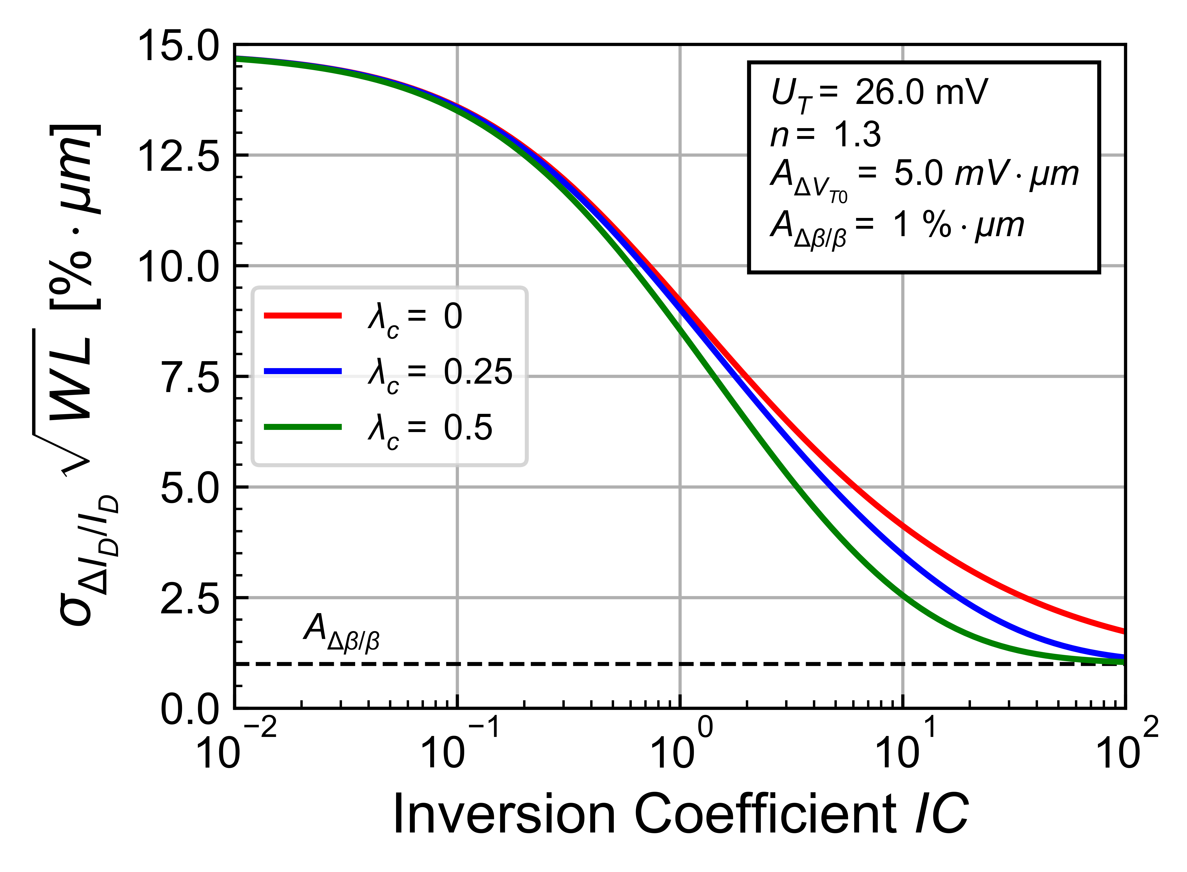
Figure 50 plots \(\sigma_{\Delta I_D/I_D} \cdot \sqrt{WL}\) versus the inversion coefficient \(IC\) for three different values of velocity saturation parameter \(\lambda_c\) that will be introduced in the next Chapter. The long-channel case corresponds to the curve for \(\lambda_c = 0\). We see that the bias dependence basically follows the \(G_m/I_D\) bias dependence which clearly shows that the best matching for currents is obtained in strong inversion. This means that current mirrors should be biased as much in strong inversion as the voltage headroom allows for obtaining the current match.
4.5.2 Gate voltage mismatch
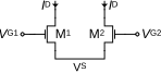
Let’s now consider two matched transistors M1 and M2 biased in saturation and having exactly the same drain current as shown in Figure 51. This configuration corresponds to a differenitialp pair. The standard deviation of the gate voltage mismatch of the two transistors is given by \[\begin{equation}\label{eqn:4:sigma_vg} \sigma_{\Delta V_G} = \sqrt{\sigma_{\Delta V_{T0}}^2 + \left(\frac{I_D}{G_m}\right)^2 \cdot \sigma_{\frac{\Delta \beta}{\beta}}^2} = \frac{1}{\sqrt{WL}} \cdot \sqrt{A_{\Delta V_{T0}}^2 + \left(\frac{I_D}{G_m}\right)^2 \cdot A_{\beta}^2}. \end{equation}\]
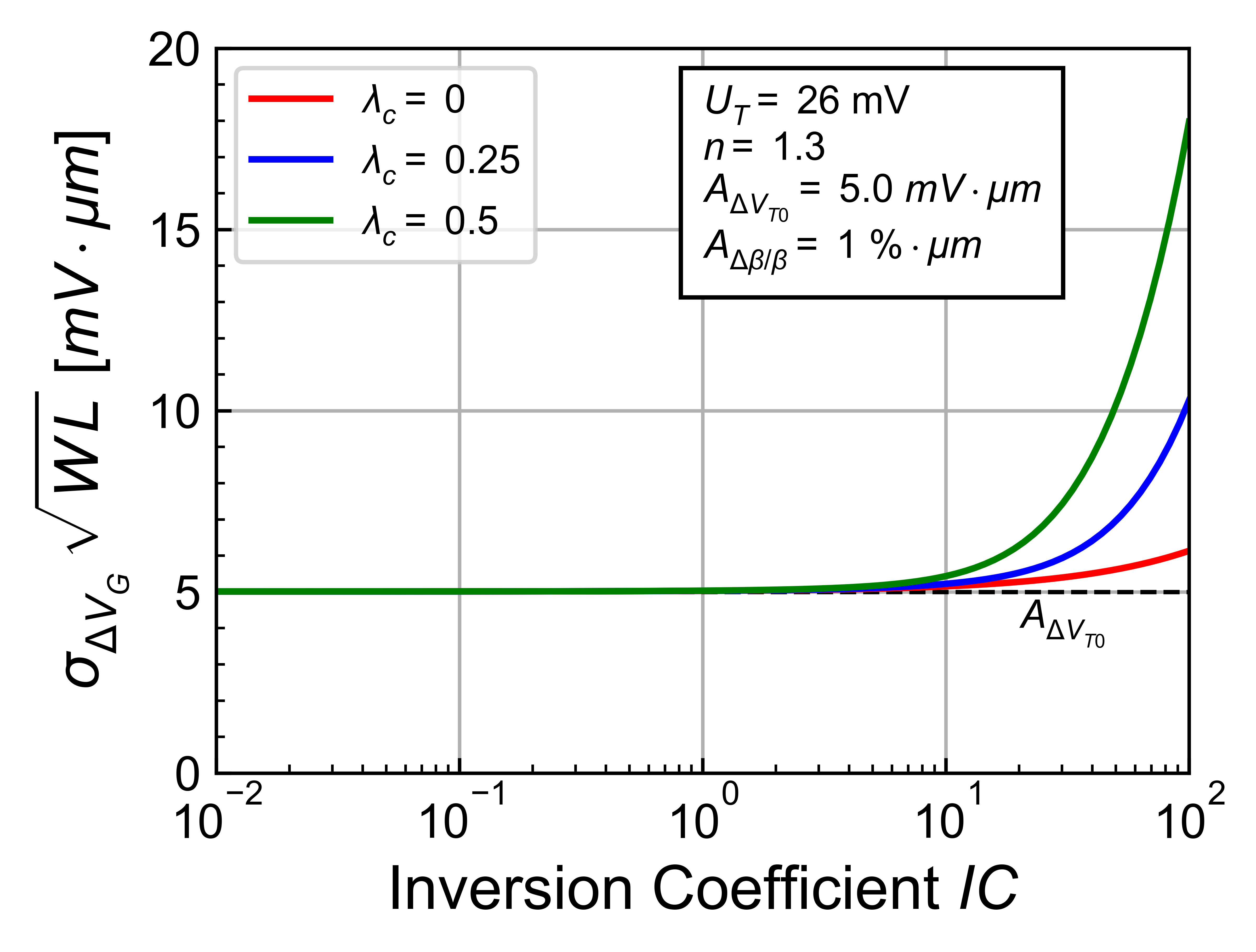
Figure 52 plots \(\sigma_{\Delta V_G} \cdot \sqrt{WL}\) versus the inversion coefficient \(IC\) for the same values of \(\lambda_c\) as in Figure 49. We see an opposite bias dependence than observed for the current mismatch. The larger the \(G_m/I_D\) ratio, the smaller the contribution of the \(\beta\)-mismatch to the overall mismatch, which reduces to the VT-mismatch \(A_{V_{T0}}\) already in moderate inversion. It is therefore better to bias differential pairs in weak inversion (eventually moderate inversion) to minimize the input-referred offset voltage.
4.5.3 Effect of nonzero source voltage on mismatch
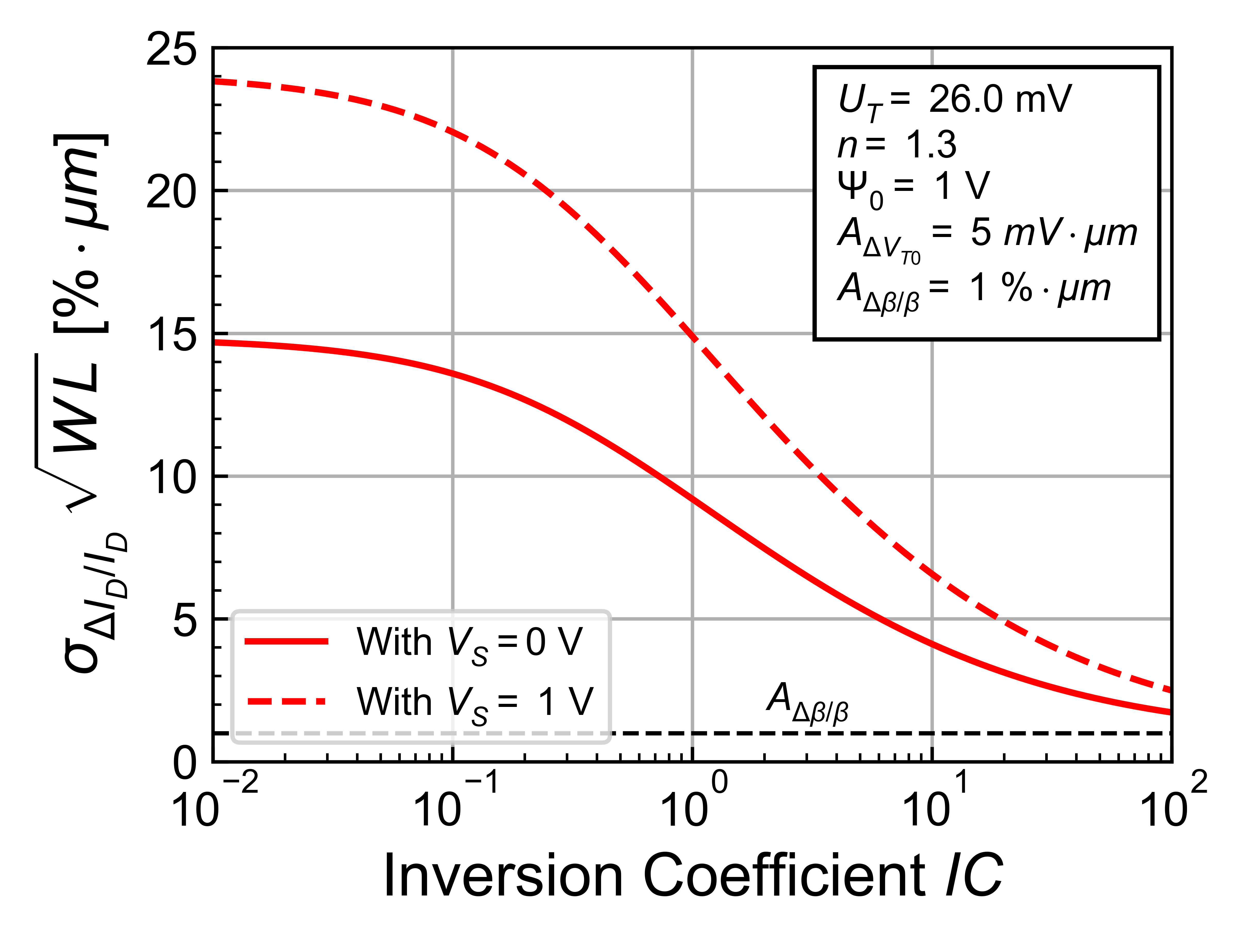
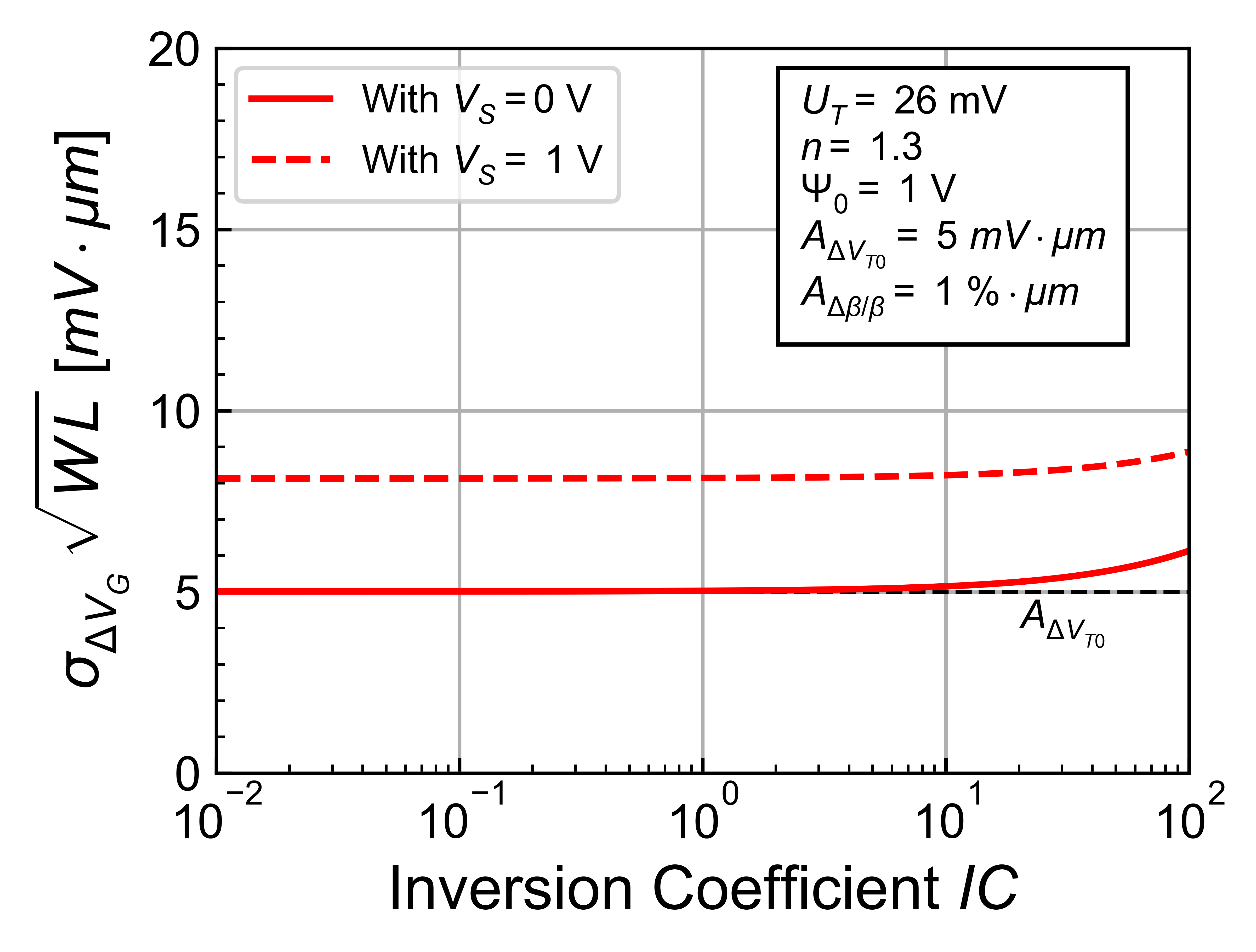
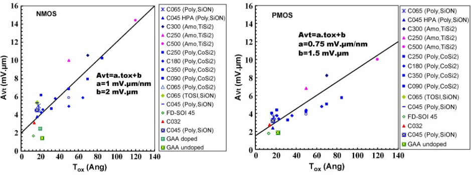
The dashed line in the plots of Figure 53 and Figure 54 illustrate the impact of a nonzero source voltage on the current mismatch and on the gate voltage mismatch due to the correlation exsisting between \(\Delta V_{T0}\) and \(\Delta n\) \[\begin{equation} \left.{\sigma_{\Delta V_G}}\right|_{V_S>0} = \sigma_{\Delta V_G} \cdot \left(1 + \frac{V_S}{2\Psi_0}\right). \end{equation}\]
It can be shown that the threshold voltage mismatch parameter \(A_{\Delta V_{T0}}\) scales with technology roughly as \[\begin{equation} A_{\Delta V_{T0}} \propto t_{ox} \cdot \sqrt[4]{N_b} \propto \frac{\sqrt[4]{\kappa}}{\kappa} \end{equation}\] where \(\kappa\) is the scaling factor by which the dimensions are divided and the doping multiplied (corresponding to the traditional Dennard scaling rules with \(\kappa > 0\)). From this Dennard scaling rule we see that the threshold mismatch parameter \(A_{\Delta V_{T0}}\) should decrease as technology are scaled down. This reduction is observed for NMOS and PMOS transistors of various CMOS bulk technologies as shown in Figure 55 [44]. It however seem to reach a minimum value of about 3 to 4 \(mV \cdot \mu m\).
4.6 References
[1]
A. Bahai, “Ultra-low energy systems: Analog to information,” in Proc. Of the european solid-state circ. Conf. (ESSCIRC), 2016, pp. 3–6.
[2]
D. Binkley, Tradeoffs and Optimization in Analog CMOS Design, 1-\(^{st}\) ed. Wiley, 2008.
[3]
W. Sansen, Analog Design Essentials, 1-\(^{st}\) ed. Springer, 2006.
[4]
A. Mangla, M. A. Chalkiadaki, F. Fadhuile, T. Taris, Y. Deval, and C. C. Enz, “Design Methodology for Ultra Low-power Analog Circuits Using Next Generation BSIM6 MOSFET Compact Model,” Microelectronics Journal, vol. 44, no. 7, pp. 570–575, 2013.
[5]
Y. S. Chauhan et al., “BSIM6: Analog and RF Compact Model for Bulk MOSFET,” IEEE Trans. on Electron Devices, vol. 61, no. 2, pp. 234–244, 2014.
[6]
C. Enz, M. A. Chalkiadaki, and A. Mangla, “Low-power Analog/RF Circuit Design Based on the Inversion Coefficient,” in Proc. Of the european solid-state circ. Conf. (ESSCIRC), 2015, pp. 202–208.
[7]
C. Enz and A. Pezzotta, “Nanoscale MOSFET Modeling for the Design of Low-power Analog and RF Circuits,” in Proc. Of the int. Conf. On mixed design of integrated circuits and systems (MIXDES), 2016.
[8]
C. Enz, F. Chicco, and A. Pezzotta, “Nanoscale MOSFET Modeling: Part 1: The Simplified EKV Model for the Design of Low-Power Analog Circuits,” IEEE Solid-State Circuits Magazine, vol. 9, no. 3, pp. 26–35, 2017.
[9]
C. Enz, F. Chicco, and A. Pezzotta, “Nanoscale MOSFET Modeling: Part 2: Using the Inversion Coefficient as the Primary Design Parameter,” IEEE Solid-State Circuits Magazine, vol. 9, no. 4, pp. 73–81, 2017.
[10]
W. Sansen, “Analog CMOS from 5 micrometer to 5 nanometer,” in IEEE int. Solid-state circuits conf. Dig. Tech. Papers (ISSCC), 2015, pp. 1–6.
[11]
W. Sansen, “Analog design procedures for channel lengths down to 20 nm,” in Electronics, circuits, and systems (ICECS), 2013 IEEE 20th international conference on, 2013, pp. 337–340.
[12]
Y. A. El-Mansy and A. R. Boothroyd, “A simple two-dimensional model for IGFET operation in the saturation region,” IEEE Transactions on Electron Devices, vol. 24, no. 3, pp. 254–262, 1977.
[13]
Y. A. El-Mansy and A. R. Boothroyd, “Authors’ reply to "Comments on ’A new approach to the theory and modeling of IGFET’s’",” IEEE Transactions on Electron Devices, vol. 25, no. 3, pp. 393–394, 1978.
[14]
B. Razavi, Design of Analog CMOS Integrated Circuits, 2-\(^{nd}\) ed. Mc Graw-Hill, 2017.
[15]
C. C. Enz and E. A. Vittoz, Charge-Based MOS Transistor Modeling - The EKV Model for Low-Power and RF IC Design, 1-\(^{st}\) ed. John Wiley, 2006.
[16]
S. M. Sze and K. K. Ng, Physics of Semiconductor Devices, 3-\(^{rd}\) ed. John Wiley, 2006. Available: https://ia601608.us.archive.org/5/items/PhysicsOfSemiconductorDevices_855/PhysicsOfSemiconductorDevices3rdEdition-S.M.SzeAndKwokK.Ng.pdf
[17]
R. M. Corless, G. H. Gonnet, D. E. G. Hare, D. J. Jeffrey, and D. E. Knuth, “On the Lambert W function,” Advances in Computational Mathematics, vol. 5, pp. 329–359, 1996.
[18]
D. Veberic, “Lambert W function for applications in physics,” Computer Physics Communications, vol. 183, no. 12, pp. 2622–2628, 2012.
[19]
H. Oguey and S. Cserveny, “MOS Modelling at Low Current Density,” ESAT, Summer Course on Process and Device Modelling, 1983.
[20]
H.-C. Han, F. Jazaeri, Z. Zhao, S. Lehmann, and C. Enz, “An improved subthreshold swing expression accounting for back-gate bias in FDSOI FETs,” Solid-State Electronics, vol. 202, p. 108608, 2023, doi: https://doi.org/10.1016/j.sse.2023.108608.
[21]
P. Jespers, The \(g_m/I_D\) Methodology, A Sizing Tool for Low-voltage Analog CMOS Circuits. in Analog circuits and signal processing. Springer, 2010.
[22]
P. G. A. Jespers and B. Murmann, Systematic Design of Analog CMOS Circuits: Using Pre-Computed Lookup Tables. Cambridge: Cambridge University Press, 2017.
[23]
A.-S. Porret, J.-M. Sallese, and C. C. Enz, “A Compact Non-Quasi-Static Extension of a Charge-Based MOS Model,” IEEE Trans. on Electron Devices, vol. 48, no. 8, pp. 1647–1654, 2001.
[24]
A. v. d. Ziel, Noise in Solid State Devices and Circuits. John Wiley, 1986.
[25]
A. S. Roy and C. C. Enz, “Compact Modeling of Thermal Noise in the MOS Transistor,” in Proceeding of the international conference on mixed design of integrated circuits and systems (MIXDES), Szczecin, Poland, 2004, pp. 71–78.
[26]
C. C. Enz and A. S. Roy, “A Comprehensive Study of Thermal Noise in the MOS Transistor,” in Symp. On fluctuations and noise - noise in devices and circuits II, F. Danneville, F. Bonani, M. J. Deen, and M. E. Levinshtein, Eds., Maspalomas, Gran Canaria Island, Spain: SPIE, May 2004, pp. 84–95.
[27]
Y. Cui, G. Niu, Y. Li, S. S. Taylor, Q. Liang, and J. D. Cressler, “On the Excess Noise Factors and Noise Parameter Equations for RF CMOS,” in 2007 topical meeting on silicon monolithic integrated circuits in RF systems, 2007, pp. 40–43.
[28]
U. Fano, “Ionization Yield of Radiations. II. The Fluctuations of the Number of Ions,” Physical Review, vol. 72, no. 1, pp. 26–29, 1947.
[29]
Y. M. Blanter and M. Büttiker, “Shot noise in mesoscopic conductors,” Physics Reports, vol. 336, no. 1, pp. 1–166, 2000.
[30]
C. Beenakker and C. Schönenberger, “Quantum Shot Noise,” Physics Today, vol. 56, no. 5, pp. 37–42, May 2003.
[31]
S. Das and J. C. Bardin, “Characterization of Shot Noise Suppression in Nanometer MOSFETs,” in 2021 IEEE MTT-s international microwave symposium (IMS), 2021, pp. 892–895.
[32]
X. Chen, C. Chen, and R. Lee, “Fast Evaluation of the High-Frequency Channel Noise in Nanoscale MOSFETs,” IEEE Transactions on Electron Devices, vol. 65, no. 4, pp. 1502–1509, 2018.
[33]
C. Xuesong, C. H. Chen, and M. J. Deen, “Short noise suppression factor for nano-scale MOSFETs working in the saturation region,” in 2017 international conference on noise and fluctuations (ICNF), 2017, pp. 1–4.
[34]
X. Chen, H. Elgabra, C. H. Chen, J. Baugh, and L. Wei, “Estimation of MOSFET Channel Noise and Noise Performance of CMOS LNAs at Cryogenic Temperatures,” in 2021 IEEE international symposium on circuits and systems (ISCAS), May 2021, pp. 1–5.
[35]
C. Enz and H.-C. Han, “The Fano Noise Suppression Factor and the \(G_{m}/I_{D}\) FoM,” in 2023 IEEE international symposium on circuits and systems (ISCAS), May 2023, pp. 1–5.
[36]
C. C. Enz, E. A. Vittoz, and F. Krummenacher, “A CMOS chopper amplifier,” IEEE Journal of Solid-State Circuits, vol. 22, no. 3, pp. 335–342, 1987.
[37]
C. C. Enz and G. C. Temes, “Circuit Techniques for Reducing the Effects of Op-amp Imperfections: Autozeroing, Correlated Double Sampling, and Chopper Stabilization,” Proceedings of the IEEE, vol. 84, no. 11, pp. 1584–1614, 1996.
[38]
M. Bucher, C. Lallement, C. Enz, F. Théodoloz, and F. Krummenacher, “The EPFL-EKV MOSFET Model Equations for Simulation.” https://github.com/chrisenz/EKV/blob/main/EKV2.6/docs/ekv_v26_rev2.pdf, 1998.
[39]
A. L. M. Worther, “1/f Noise and Germanium Surface Properties,” in Semiconductor surface physics, R. H. Kingston, Ed., Philadelphia: University of Pennsylvania Press, 1957, pp. 207–228.
[40]
F. N. Hooge, “1/f Noise,” Physica, vol. 83B, pp. 14–23, 1976.
[41]
X. Li and L. K. J. Vandamme, “An Explanantion of 1/f Noise in LDD MOSFETs from the Ohmic Region to Saturation,” Solid-State Electronics, vol. 36, no. 11, pp. 1515–1521, 1993.
[42]
M. J. M. Pelgrom, A. C. J. Duinmaijer, and A. P. G. Welbers, “Matching properties of MOS transistors,” IEEE Journal of Solid-State Circuits, vol. 24, no. 5, pp. 1433–1439, 1989.
[43]
K. R. Lakshmikumar, R. A. Hadaway, and M. A. Copeland, “Characterisation and modeling of mismatch in MOS transistors for precision analog design,” IEEE Journal of Solid-State Circuits, vol. 21, no. 6, pp. 1057–1066, 1986.
[44]
C. M. Mezzomo, A. Bajolet, A. Cathignol, R. Di Frenza, and G. Ghibaudo, “Characterization and Modeling of Transistor Variability in Advanced CMOS Technologies,” IEEE Transactions on Electron Devices, vol. 58, no. 8, pp. 2235–2248, 2011, doi: 10.1109/TED.2011.2141140.