Analog Integrated Circuits Design using the Inversion Coefficient
Preview Edition
Licensing
This document is licensed under the Creative Commons License CC BY-NC-SA 
6 The Concept of inversion coefficient
6.1 Introduction
In this Chapter, we will show that the inversion coefficient \(IC\) can replace the old-fashioned overdrive voltage \(V_G-V_{T0}\) or \(V_{GS}-V_T\) as the main variable for sizing a given transistor according to some specifications. The overdrive voltage \(V_G-V_{T0}\) works mostly in strong inversion, but is not very practical outside strong inversion because it becomes zero in moderate inversion or even negative in weak inversion. It is therefore better to use the inversion coefficient \(IC\) because it covers the whole operating range of a transistor in saturation, from weak to strong inversion through moderate inversion.
We will show that using the inversion coefficient allows to explore the design space for sizing a single transistor according to some specifications. It can also help exploring basic trade-offs and finding optimum operating point using appropriate figure-of-merits.
6.2 The \(G_m/I_D\) design methodology
6.2.1 The inversion coefficient
The optimization of analog circuit for low-power operation often leads to relations involving the \(G_m/I_D\) ratio. The \(G_m/I_D\) ratio is a figure-of-merit (FoM) which tells how much transconductance you get for a given current at a certain operating point characterized by the inversion coefficient \(IC\). The \(G_m/I_D\) design methodology was therefore created for the design of ultra low-power analog circuits covering the whole range of bias ranging from weak inversion to strong inversion.
The \(G_m/I_D\) ratio can be used directly as the main design variable to set the operating point of a transistor. As discussed below, we prefer to use the inversion coefficient because it is proportional to the drain current in saturation as stated by the its definition given by \[\begin{equation} IC \triangleq \frac{\left.I_D\right|_{saturation}}{I_{spec}}, \end{equation}\] where the specific current \(I_{spec}\) is defined as \[\begin{equation} I_{spec} \triangleq I_{spec\Box} \cdot \frac{W}{L}. \end{equation}\] The specific current per square \(I_{spec\Box}\) is an important process parameter defined as \[\begin{equation} I_{spec\Box} \triangleq 2n \cdot \mu \cdot C_{ox} \cdot U_T^2. \end{equation}\] with \(U_T \triangleq k_B\,T/q\) the thermodynamic voltage. Typical values of \(I_{spec\Box}\) for a 28 nm bulk CMOS process are given in .

The different regions of operation can then be defined from the inversion coefficient as illustrated in Figure 1 and defined below \[\begin{equation} \begin{aligned} &IC \leq 0.1 &&\textsf{weak inversion (WI)},\\ 0.1 <& IC \leq 10 &&\textsf{moderate inversion (MI)},\\ 10 <& IC &&\textsf{strong inversion (SI).} \end{aligned} \end{equation}\] For \(IC<1\), the transistor is in subthreshold.
6.2.2 \(G_m/I_D\) or \(IC\) as main design parameter?
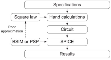
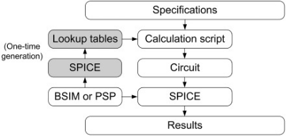
Figure 2 (a) shows the simplified design flow for analog circuits [1]. It starts with the circuit specifications, followed by some analysis to link the specs to the circuits parameters (currents, voltages, transconductances, etc…). The analysis is often carried using the simplistic quadratic strong inversion model to size the transistors and set the bias currents of the chosen circuit. Spice simulation are then performed which are often far from the desired specifications. The reason for this is that the simple quadratic model used in the preliminary analysis phase is a poor approximation of the model that is actually used in the simulator, leading to significant discrepancy between the initial hand calculations and the simulations.
As shown in Figure 2 (b), Jespers and Murmann are proposing to use directly the \(G_m/I_D\) variable as the main design parameter combined with look-up tables that are computed from the compact model available in the physical design kit (PDK) for a specific technology [1]. The hand calculations are then replaced by MatLab scripts to size the various transistors and set the bias currents of the designed circuit according to specs. In this way, the simulations results will be much closer to the results obtained from the calculation scripts.
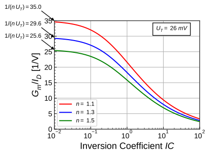
Figure 3 shows the \(G_m/I_D\) versus \(IC\) plot for a long-channel transistor without normalizing the y-axis which now appears in \(1/V\). Contrary to the normalized version, \(G_m/I_D\) depends on the slope factor \(n\) and on temperature through the thermodynamic voltage \(U_T\). As shown in Figure 3, the use of the \(G_m/I_D\) as the main design parameter is fine in the region of moderate inversion, however it is not convenient in weak inversion because \(G_m/I_D\) saturates to \(n\,U_T\) as the operating point moves towards weak inversion. This means that a slight variation in \(G_m/I_D\) can significantly change the inversion coefficient. On the other hand it is maybe more convenient in strong inversion because it includes the effect of velocity saturation. Since the EKV model gives a simple analytical expression of \(G_m/I_D\) in terms of \(IC\), it is actually better to use directly the inversion coefficient \(IC\) as the main design parameter instead of \(V_G-V_{T0}\) or directly \(G_m/I_D\). The \(IC\) design methodology will be illustrated by many examples in Chapter ???. We also will show in Section 6.3 that the inversion coefficient helps exploring trade-offs and finding optima using figures-of-merit.
6.2.3 Specific current extractor
The specific current is not a theoretical abstraction. It can actually be extracted for a given type of transistor from a given technology. If we are able to extract \(I_{spec\Box}\) for each type of transistor we can then set the inversion coefficient of each transistor using a bias current that is proportional to this \(I_{spec\Box}\).
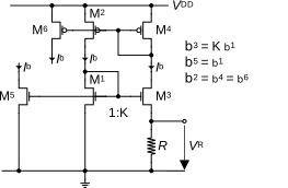
Note that this current reference also works when M1 and M3 are biased in strong inversion.
The specific current extractor is based on the Vittoz current reference shown in Figure 4 which provides a reference current for biasing transistors in weak inversion [2]. It is made of transistors M1 and M3 which are biased in weak inversion with M3 made \(K\)-times larger than M1. Transistors M2-M4 are biased in strong inversion and form a current mirror imposing that the current in M1 is equal to the current flowing in M3. Because M3 is made \(K\)-times larger than M1, it needs less gate-to-source voltage for driving the same current than M1 and a voltage \(V_R\) develops across resistance \(R\). We now will show that this reference voltage \(V_R\) is actually proportional to absolute temperature or PTAT.
To analyze this circuit we first express the currents of M1 and M3 assuming that M1 and M3 have the same threshold voltage \(V_{T0}\) and slope factor \(n\) \[\begin{align} I_{D1} &= I_{spec1} \cdot e^{\frac{V_P}{U_T}} \cong I_{spec1} \cdot e^{\frac{V_G-V_{T0}}{n\,U_T}},\label{eqn:sce_id1}\\ I_{D3} &= I_{spec3} \cdot e^{\frac{V_P}{U_T}} \cdot e^{-\frac{V_R}{U_T}} \cong I_{spec3} \cdot e^{\frac{V_G-V_{T0}}{n\,U_T}} \cdot e^{-\frac{V_R}{U_T}},\label{eqn:sce_id3} \end{align}\] where \(V_P\) and \(V_G\) are the pinch-off and gate voltages of M1 and M3. Assuming that M2 and M4 are perfectly matched then \(I_{D1} = I_{D3} = I_b\). Since M3 is made \(K\) times larger than M1, \(I_{spec3} = K \cdot I_{spec1}\). Equating \(\eqref{eqn:sce_id1}\) and \(\eqref{eqn:sce_id3}\) leads to \[\begin{equation} K = e^{\frac{V_R}{U_T}}. \end{equation}\] The voltage \(V_R\) is therefore a PTAT voltage given by \[\begin{equation}\label{eqn:sce_VR} V_R = U_T \cdot \ln(K) \end{equation}\] and the reference current is then given by \[\begin{equation} I_b = \frac{U_T}{R} \cdot \ln(K). \end{equation}\] The temperature dependence of \(I_b\) finally depends on the temperature behavior of the chosen resistor \(R\). Imposing this current to a transistor biased in weak inversion will make its source transconductance \(G_{ms}\) inversely proportional to the resistance \(R\) according to \(G_{ms} = I_b/U_T = \ln(K)/R\). If we can assume that the temperature dependence of \(R\) is negligible, the transconductance becomes to first order independent to temperature.
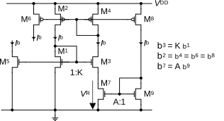
H. Oguey proposed to replace the resistor by a MOSFET biased in the linear region [3]. The corresponding circuit is shown in Figure 5, where M6 replaces the resistor of the Vittoz current reference. M7 and M9 are biased in strong inversion and M7 is made \(A\)-times larger than M9 to force it to operate in the linear region. Since M7 and M9 share the same gate voltage they have the same pinch-off voltage \(V_{P7}=V_{P9}\). The current of M7 and M9 are given by \[\begin{align} I_{D7} &= I_b = A \cdot I_{spec7} \cdot \left[\left(\frac{V_{P7}}{2 U_T}\right)^2 - \left(\frac{V_{P7}-V_R}{2 U_T}\right)^2\right],\label{eqn:ID7}\\ I_{D9} &= I_b = I_{spec9} \cdot \left(\frac{V_{P7}}{2 U_T}\right)^2.\label{eqn:ID9} \end{align}\] Equating \(\eqref{eqn:ID7}\) and \(\eqref{eqn:ID9}\) and solving for \(I_b\) results in \[\begin{equation}\label{eqn:oguey_ib1} I_b = I_{spec9} \cdot \left(\frac{A\,\ln(K)}{2}\right)^2 \cdot \left(1 + \sqrt{1+\frac{1}{A}}\right)^2. \end{equation}\] If \(A\) can be considered much larger than 1, \(\eqref{eqn:oguey_ib1}\) simplifies to \[\begin{equation}\label{eqn:oguey_ib2} I_b \cong I_{spec9} \cdot \left[A \cdot \ln(K)\right]^2. \end{equation}\] Equation \(\eqref{eqn:oguey_ib2}\) shows that \(I_b\) is proportional to \(I_{spec9}\). Since \(I_{spec9}=I_{spec7}/A\), \(\eqref{eqn:oguey_ib2}\) can also be written as \[\begin{equation}\label{eqn:oguey_ib3} I_b \cong I_{spec7} \cdot A \cdot [\ln(K)]^2. \end{equation}\] which shows that \(I_b\) is also proportional to \(I_{spec7}\).
The circuit of Figure 5 provides a reference current that is proportional to the specific current of a reference transistor, for example M9 or M7 which are in strong inversion and saturation or M1 which is in weak inversion and saturation. This current reference enables to precisely set the inversion coefficient of any n-channel transistor by choosing an appropriate series and parallel combination of the reference transistor. Of course an additional p-channel current reference is needed for biasing p-channel transistors.
Note that for the reference current to become independent of the temperature would require the mobility to be inversely proportional to the square of the temperature to compensate for the \(U_T^2\) term present in \(I_{spec}\). Although mobility increases when reducing the temperature, it does not scale exactly as \(T^{-2}\) and therefore the reference current is slightly temperature dependent.
We will show in the next Section how this current reference can be used to bias a transistor of the same type at a given inversion coefficient.
6.2.4 Ratio-based design
Any n-channel transistor Mx can be operated at a given inversion coefficient \(IC_x\) by means of a weighted copy of the current \(I_b\) provided by the reference current circuit of Figure 5. For a transistor Mx that has to be biased in weak inversion, it is best to use transistor M1 of the specific current extractor of Figure 5 as a reference transistor. The drain current of transistor Mx can be set to \(N\) times the bias current \[\begin{equation} I_x = N \cdot I_b \end{equation}\] which can be written as \[\begin{equation} IC_x \cdot I_{specx} = N \cdot IC_1 \cdot I_{spec1} \end{equation}\] hence \[\begin{equation} IC_x \cdot \frac{W_x}{L_x} = N \cdot IC_1 \cdot \frac{W_1}{L_1} \end{equation}\] where \(W_x\) and \(L_x\) are the width and length of transistor Mx and \(IC_1\), \(W_1\) and \(L_1\) are the inversion coefficient, width and length of transistor M1 of the specific current extractor of Figure 5. The transistor \(W/L\) ratio required to bias Mx at an inversion coefficient \(IC_x\) is then given by \[\begin{equation} \frac{W_x}{L_x} = N \cdot \frac{IC_1}{IC_x} \cdot \frac{W_1}{L_1}. \end{equation}\]
A similar rule applies for biasing a transistor more in strong inversion taking M7 as the reference transistor. Note that this biasing technique is independent of the particular value of the threshold voltage (as long as all the transistors remain in saturation).
6.2.5 Circuit design and transistor sizing
The designer needs to size each transistor of a chosen circuit in order to achieve the circuit specifications (gain, bandwidth, noise, linearity,…). Sizing each transistor actually means choosing its operating point which can be done by setting its inversion coefficient \(IC\) selecting the appropriate
- drain current \(I_D\),
- transistor width \(W\) and
- transistor length \(L\).
The specifications for each device is often related to the gate transconductance \(G_m\) which is linked to \(IC\) and the \(W/L\) ratio by \[\begin{equation}\label{eqn:Gm_gms_IC} G_m = \frac{G_{ms}}{n} = \frac{G_{spec}}{n} \cdot g_{ms}(IC) = \frac{I_{spec}}{n\,U_T} \cdot g_{ms}(IC) = \frac{I_{spec\Box}}{n\,U_T} \cdot \frac{W}{L} \cdot g_{ms}(IC) \end{equation}\] where the normalized source transconductance including the effect of velocity saturation is given by \(\eqref{eqn:gms_ic_vs}\) which is repeated here for convenience \[\begin{equation*} g_{ms} = \frac{\sqrt{4IC+1+(\lambda_c\,IC)^2}-1}{2+\lambda_c^2\,IC}. \end{equation*}\]
A generic design flow based on the inversion coefficient can be sketched as follows:
- Determine \(G_m\) from the design objectives (for example from the DC gain, bandwidth, gain-bandwidth product or thermal noise).
- Pick \(IC\)
- strong inversion with \(IC > 10\) for high speed (high \(F_t\)) and high linearity, remembering that the maximum \(IC\) is limited by the available voltage headroom.
- weak inversion with \(IC < 0.1\) for low-power and low-voltage thanks to its minimum saturation voltage \(V_{DS_{sat}}\), but slow, large area and highly nonlinear.
- moderate inversion with \(0.1 \leq IC \leq 10\) as a good trade-off between speed, area and linearity. This is often a good starting point if it is not obvious to choose strong or weak inversion.
- Pick \(L\)
- Short channel for high speed (high \(F_t\)).
- Non-minimum length as a good trade-off for avoiding degrading the intrinsic DC gain.
- Long channel for high intrinsic gain.
- Calculate \(L_{eff}=L+\Delta L\) and \(\lambda_c = L_{sat}/L_{eff}\) to determine \(G_m/I_D\) from \(IC\) according to \[\begin{equation*} \frac{g_{ms}}{i_d} = \frac{G_{ms} \cdot U_T}{I_D} = \frac{G_m \cdot n\,U_T}{I_D} = \frac{\sqrt{4IC+1+(\lambda_c\,IC)^2}-1}{IC\,(2+\lambda_c^2\,IC)} \end{equation*}\]
- Determine \(I_D\) from \(G_m/I_D\) and target \(G_m\) according to \[\begin{equation*} I_D = \frac{G_m \cdot n \cdot U_T}{g_{ms}/i_d}. \end{equation*}\]
- Determine \(I_{spec}\) from \(IC\) and \(I_D\) according to \[\begin{equation*} I_{spec} = \frac{I_D}{IC}. \end{equation*}\]
- Determine \(W/L\) from \(I_{spec}\) according to \[\begin{equation*} WoverL = \frac{W_{eff}}{L_{eff}} = \frac{I_{spec}}{I_{spec\Box}}. \end{equation*}\]
- Determine \(W\) from \(L\) \[\begin{equation*} W_{eff} = WoverL \cdot L_{eff} \end{equation*}\] and \(W=W_{eff}-\Delta W\).
Parameter \(\Delta W\) and \(\Delta L\) are process parameters used to calculate the effective width \(W_{eff}\) and effective length \(L_{eff}\) according to \[\begin{align*} W_{eff} &= W+\Delta W,\\ L_{eff} &= L+\Delta L. \end{align*}\] Note that \(\Delta L\) is usually negative meaning that the effective length \(L_{eff}\) is smaller than the drawn length \(L\). The effective width \(W_{eff}\) can be smaller or larger than than the drawn width \(W\) depending on the type of transistor and technology.
An alternative design flow is presented below in the case both the current \(I_D\) and transconductance \(G_m\) are imposed.
- We first calculate the \(G_m/I_D\) ratio with \[\begin{equation*} \frac{g_{ms}}{i_d} = \frac{G_{ms} \cdot U_T}{I_D} = \frac{G_m \cdot n\,U_T}{I_D}. \end{equation*}\]
- Neglecting velocity saturation, we can then derive \(IC\) as \[\begin{equation*} IC = \frac{1-g_{ms}/i_d}{g_{ms}/i_d}. \end{equation*}\]
- Determine \(I_{spec}\) from \(IC\) and \(I_D\) according to \[\begin{equation*} I_{spec} = \frac{I_D}{IC}. \end{equation*}\]
- Determine \(W/L\) from \(I_{spec}\) according to \[\begin{equation*} WoverL = \frac{W_{eff}}{L_{eff}} = \frac{I_{spec}}{I_{spec\Box}}. \end{equation*}\]
- Pick \(L\)
- Short channel for high speed (high \(F_t\)).
- Non-minimum length as good trade-off.
- Long channel for high intrinsic gain.
- Determine \(W\) from \(L_{eff}=L+\Delta L\) \[\begin{equation*} W_{eff} = WoverL \cdot L_{eff} \end{equation*}\] and finally the drawn width \(W=W_{eff}+\Delta W\).
The above sizing flows need then to be fine tuned by simulations.
We now will show how we can use figures-of-merit to explore different trade-offs for finding the optimum operating point or inversion coefficient.
6.3 Figures-of-merit (FoMs) as design guidelines
Figures-of-merit (FoMs) can guide the designer in the design space to converge to an optimum solution. There many FoMs that can be defined for a single transistor, including:
- The current efficiency \(G_m/I_D\) stating how much transconductance you get for a given current.
- The transit frequency \(F_t=G_m/(2\pi C_G)\), evaluating the maximum frequency above which there is no more gain.
- The intrinsic gain or self gain \(G_m/G_{ds}\) giving the transistor DC voltage gain.
- The thermal noise excess factor \(\gamma_n = G_m \cdot R_{ninth}\) stating how much thermal noise you get for a given transconductance \(G_m\).
- The minimum noise factor \(F_{min}\), giving the minimum noise factor achievable under noise matching condition.
Other FoMs can be defined exploiting other trade-offs like for example the \(G_m/I_D \cdot F_t\). We will examine each of these FoM below.
6.3.1 The transconductance efficiency \(G_m/I_D\)
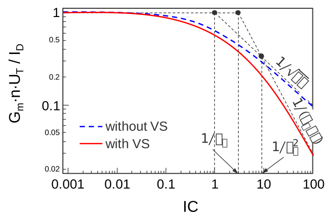
The transconductance efficiency \(G_m/I_D\) FoM is one of the most important performance metric for analog circuit design. It is a measure of how much transconductance is produced for a given bias current and is a function of \(IC\) only (eventually \(\lambda_c\) for short-channel devices). The transconductance efficiency (or its inverse) appears in many expressions related to the power optimization of analog circuits. Examples will be given in Chapter ???.
In the normalized form, the transconductance efficiency is defined as the ratio of the actual gate transconductance in saturation obtained at a given \(IC\) to the maximum transconductance \(G_m = I_D/(n\,U_T)\) reached in weak inversion [7] [8] \[\begin{equation}\label{eqn:gms_id_def} \frac{g_{ms}}{IC} = \frac{G_m \cdot n\,U_T}{I_D} = \frac{\sqrt{4IC+1+(\lambda_c IC)^2}-1}{IC \cdot (2+\lambda_c^2 IC)} = \begin{cases} 1 & \textsf{WI and sat.}\\ \frac{1}{\lambda_c IC} & \textsf{SI and sat. (with VS)}. \end{cases} \end{equation}\] The expression in \(\eqref{eqn:gms_id_def}\), which is continuous from weak to strong inversion and includes the effect of velocity saturation, is plotted in Figure 6. The figure shows the behavior of \(g_{ms}/IC\) for long-channel devices in which velocity saturation is absent which scales as \(1/\sqrt{IC}\) in strong inversion (dashed blue curve). For short-channel devices subject to velocity saturation, the drain current becomes a linear function of the gate voltage, independent of the transistor length. Hence, the transconductance becomes independent of the current and of the length. Since \(G_m\) becomes independent of \(I_D\) or of \(IC\), the \(G_m/I_D\) curve scales like \(1/(\lambda_c IC)\) in strong inversion instead of \(1/\sqrt{IC}\) when velocity saturation is absent. In essence, the effect of velocity saturation is to degrade the transconductance efficiency in strong inversion, meaning that more current is required to reach the same transconductance obtained without velocity saturation. Nevertheless, irrespective of the channel length, \(G_m/I_D\) remains invariant (i.e. \(g_{ms}/IC=1\)) in weak inversion, since short-channel effects (SCE), including velocity saturation, have the same effect on \(G_m\) than on \(I_D\) simply because \(G_m\) is proportional to \(I_D\) in weak inversion.
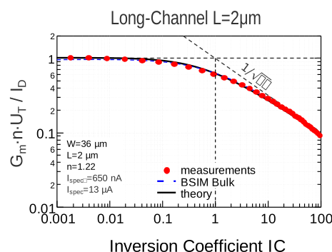
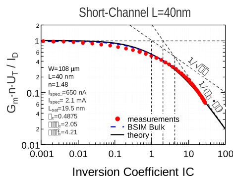
The current efficiency \(G_m/I_D\) FoM has been measured on n-channel transistors from a 40 nm bulk CMOS and is represented in normalized for in Figure 7. Figure 7 (a) compares the measured \(G_m/I_D\) FoM of a wide and long channel device (\(L=2\,\mu m\)) (red circles) to the analytical expression (black line) and to the simulation results from the BSIM-bulk compact model (dashed blue line). We see that the simple model without velocity saturation (\(\lambda_c=0\)) perfectly matches the measured data and the simulations over 5 decades of inversion coefficient. Figure 7 (b) shows the \(G_m/I_D\) measured on a wide and short device (\(L=40\,nm\)) which highlights the effect of velocity saturation in strong inversion where the \(G_m/I_D\) decreases as \(1/(\lambda_c IC)\). The simple expression of the normalized \(G_m/I_D\) fits the data very well for \(\lambda_c = 0.5\). This value is extracted from the inversion coefficient corresponding to the intersection of the \(1/(\lambda_c IC)\) asymptote and the horizontal unity line.
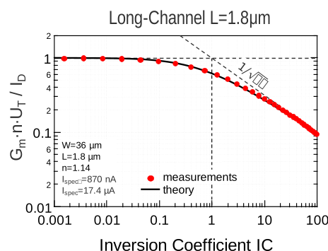
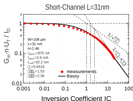
Figure 8 shows measurements of the \(G_m/I_D\) FoM made on NMOS devices from a 28 nm bulk CMOS technology. Figure 8 (a) corresponds to a wide and long channel (\(L=1.8\,\mu m\)), whereas Figure 8 (b) corresponds to a wide and short channel transistor (\(L=31\,nm\)). We again see a very good match between the simple model and the measurements. We also see that as expected, the parameter \(\lambda_c\) has increased to 0.65 compared to 0.5 for the 40 nm devices.
6.3.2 The transit frequency \(F_t\)
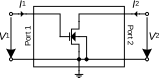
As shown in Figure 9, the transit frequency \(F_t\) is defined from the small-signal current gain \(h_{21}\) \[\begin{equation} h_{21} \triangleq \left.\frac{I_2}{I_1}\right|_{V_2=0} = \frac{Y_{21}}{Y_{11}} = \frac{G_m - j\omega (C_m+C_{GD})}{j\omega C_G}, \end{equation}\] where \(I_1\) and \(I_2\) are the small-signal currents at port 1 (gate) and port 2 (drain), respectively. \(C_G\) is the total capacitance seen at the gate, \(C_m\) is the gate transcapacitance and \(C_{GD}\) the gate-to-drain capacitance. For \(\omega \ll G_m/(C_m+C_{GD})\), \(h_{21}\) can be approximated as \[\begin{equation} h_{21} \cong \frac{G_m}{j\omega\,C_G} = \frac{\omega_t}{j\omega}. \end{equation}\] The transit frequency \(F_t\) is defined as the frequency at which the extrapolated small-signal current gain \(h_{21}\) of the transistor in CS configuration falls to unity [9]. \(F_t\) is a widely used metric for characterizing the high-frequency behavior of a MOSFET because many performance, such as the gain at RF and the minimum noise factor, are directly linked to \(F_t\) [9]. A good approximation of \(F_t\) is given by [9] [10] \[\begin{equation} F_t = \frac{\omega_t}{2\pi} = \frac{1}{2\pi} \cdot \frac{G_m}{C_G} \end{equation}\] where the total gate capacitance \(C_G=C_{Gi}+C_{Ge}\) can be split into the intrinsic capacitance \(C_{Gi}\), which is linked to the mobile charges in the channel and the extrinsic capacitance \(C_{Ge}\). The intrinsic gate capacitance is bias dependent and is therefore proportional to the total gate oxide capacitance \(W \cdot L \cdot C_{ox}\).
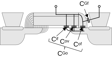
As shown in Figure 10, the extrinsic gate capacitance \(C_{Ge}\) is made of the overlap capacitance \(C_{Go}\) and the fringing-field capacitance \(C_{Gf}\) and scales with the transistor width \(W\) \[\begin{equation} C_{Ge} = C_{Go} + C_{Gf} = W \cdot C_{GeW}, \end{equation}\] where \(C_{GeW}\) is the total extrinsic capacitance per unit width.
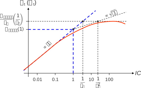
Since both \(G_m\) and \(C_{Gi}\) are bias dependent, \(F_t\) is bias dependent too. Its variation with respect to \(IC\) is shown in Figure 11. In weak inversion, the mobile charges are few and the intrinsic gate capacitance is negligible compare to the extrinsic capacitance so that \(C_G \cong C_{Ge}\). The bias dependence in weak inversion is therefore mostly coming from \(G_m\). Since in weak inversion \(G_m \propto I_D\) and hence \(G_m \propto IC\), \(\omega_t\) is therefore also proportional to \(IC\).
The transit frequency can be written in terms of the inversion coefficient as \[\begin{equation}\label{eqn:omegat1} \omega_t = \frac{G_m}{C_G} = \frac{G_{spec}}{n \cdot W \cdot L \cdot C_{ox}} \cdot \frac{g_{ms}(IC)}{c_{Gi} + \frac{C_{Ge}}{W \cdot L \cdot C_{ox}}} \end{equation}\] where the normalized source transconductance in saturation is given by \[\begin{equation}\label{eqn:gms_ic} g_{ms}(IC) = \frac{\sqrt{4IC+1+(\lambda_c IC)^2}-1}{2+\lambda_c^2 IC} = \begin{cases} \frac{\sqrt{4IC+1}-1}{2} & \textsf{all regions without VS}\\ IC & \textsf{WI}\\ \sqrt{IC} & \textsf{SI without VS}\\ \frac{1}{\lambda_c} & \textsf{SI with VS ($\lambda_c \cdot IC \gg 1$)}. \end{cases} \end{equation}\] \(c_{Gi}\) is the normalized intrinsic gate capacitance, which in saturation is given by \[\begin{equation} c_{Gi} \triangleq \frac{C_{Gi}}{W \cdot L \cdot C_{ox}} = \begin{cases} 1-\tfrac{1}{n} & \textsf{WI}\\ 1-\tfrac{1}{3n} & \textsf{SI}. \end{cases} \end{equation}\]
Replacing \(G_{spec}\) in \(\eqref{eqn:omegat1}\) results in \[\begin{equation}\label{eqn:omegat2} \omega_t = \omega_{spec} \cdot \frac{g_{ms}(IC)}{c_{Gi} + \frac{C_{Ge}}{W \cdot L \cdot C_{ox}}}, \end{equation}\] where the specific frequency \(\omega_{sec}\) is defined as \[\begin{equation} \omega_{spec} = \frac{2\mu \cdot U_T}{L^2}. \end{equation}\] Note that \(\omega_{sec}\) actually scales as \(1/L^2\).
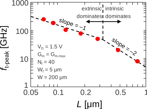
For short-channel devices, the gate capacitance is dominated by the extrinsic part and hence independent of \(IC\) \[\begin{equation}\label{eqn:cg} c_G \triangleq \frac{C_G}{W \cdot L \cdot C_{ox}} = c_{Gi} + \frac{C_{Ge}}{W \cdot L \cdot C_{ox}} \cong \frac{C_{Ge}}{W \cdot L \cdot C_{ox}} = \frac{C_{GeW}}{L \cdot C_{ox}}. \end{equation}\] Introducing \(\eqref{eqn:cg}\) into \(\eqref{eqn:omegat2}\) results in \[\begin{equation}\label{eqn:omegat3} \omega_t \cong \omega_{spec} \cdot \frac{L \cdot C_{ox}}{C_{GeW}} \cdot g_{ms}(IC) = \frac{2\mu \cdot U_T}{L} \cdot \frac{C_{ox}}{C_{GeW}} \cdot g_{ms}(IC). \end{equation}\] Equation \(\eqref{eqn:omegat3}\) shows that when the extrinsic capacitance dominates the gate capacitance, the bias dependency of \(\omega_t\) follows that of \(g_{ms}\) and \(\omega_t\) only scales as \(1/L\) compared to \(\eqref{eqn:omegat2}\) which scales as \(1/L^2\). This change of scaling with \(L\) was observed already in 1996 by Momose [12]. As shown in Figure 12, for \(L>250\,nm\), \(F_t\) scales as \(1/L^2\) and for \(L<250\,nm\), \(F_t\) only scales as \(1/L\). This is also observed in more recent technologies as shown in Figure 13 which presents the transit frequency measured on devices from a 45 nm and 32 nm bulk CMOS processes [13] [14]. Figure 13 (a) shows that the transit frequency measured on a 45 nm bulk CMOS technology indeed scales as \(1/L\). Figure 13 (b) shows the transit frequency measured on a 32 nm bulk CMOS process versus the gate length which scales as \(1/L^2\) above 180 nm and as \(1/L\) below.
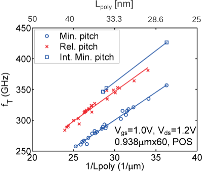
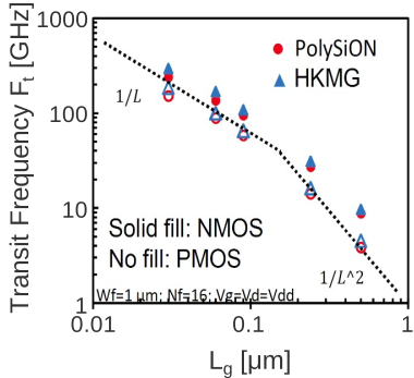
Similarly to the \(G_m/I_D\) characteristic, \(\omega_t\) can be normalized as shown in Figure 11 to the specific transit frequency \(\omega_{tspec}\) defined as the value of \(\omega_t\) on the weak inversion asymptote corresponding to \(IC=1\) [7] [11] \[\begin{equation} \omega_{tspec} \triangleq \left.\omega_t\right|_{\textsf{WI at $IC=1$}} = \frac{\omega_{spec}}{c_{Gi} + \frac{C_{Ge}}{W \cdot L \cdot C_{ox}}} \cong \frac{2\mu \cdot U_T}{L} \cdot \frac{C_{ox}}{C_{GeW}}. \end{equation}\] In this way, the normalized transit frequency \(\Omega_t \triangleq \omega_t/\omega_{tspec}\) turns out to be equal to \(g_{ms}\) which is given by \(\eqref{eqn:gms_ic}\). As illustrated in Figure 11, in strong inversion and under velocity saturation (i.e. for \(1/\lambda_c^2 < IC\)), \(\omega_t\) (or \(\Omega_t\) in normalized form) saturates to \(\omega_{tspec}/\lambda_c\) (or \(1/\lambda_c\) in normalized form). When increasing the channel length, i.e. for lower values of \(\lambda_c\), the value of \(IC\) at which velocity saturation starts, moves to higher values and there is a region between \(IC=1\) and \(IC=1/\lambda_c^2\) where \(\omega_t\) follows the strong inversion asymptote \(\sqrt{IC}\).
Note that once the velocity saturation parameter \(\lambda_c\) is extracted from the \(G_m/I_D\) characteristic as described in [7], it is therefore easy to assess the peak \(\omega_t\) for a given technology from \(\omega_{tspec}\). Indeed for short-channel devices \(C_{Gi} \ll C_{Ge}\) and \(\omega_{tspec}\) can be written as \[\begin{equation} \omega_{tspec} \cong \frac{I_{spec\Box}}{n\,U_T \cdot C_{GeW} \cdot L}. \end{equation}\] The peak transit frequency is then given by \[\begin{equation} \omega_{tpeak} = \frac{\omega_{tspec}}{\lambda_c} \cong v_{sat} \cdot \frac{C_{ox}}{C_{GeW}}. \end{equation}\] which shows that surprisingly \(\omega_{tpeak}\) does not scale as \(1/L\) anymore [7] [11]. This means that the only way to increase \(\omega_{tpeak}\) is to increase \(C_{ox}\) but without increasing \(C_{GeW}\) [7] [11]. This observation could explain the recent slow-down of the peak transit frequency progression witnessed when FinFET were first introduced.
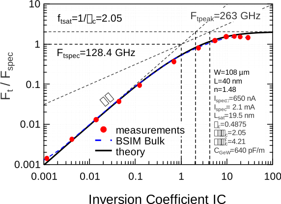
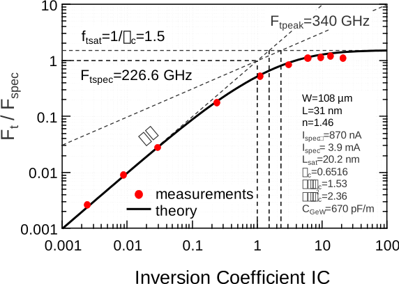
Figure 14 (a) and Figure 14 (b) show the normalized \(F_t\) versus the inversion coefficient \(IC\) measured on nMOS transistors from a 40 nm and 28 nm bulk CMOS technology, respectively. The measurements are compared to the simple analytical expression \(\eqref{eqn:omegat3}\). We see a very good match except at higher value of \(IC\) where the measurements tends to decrease. This is due to the fact that at such high \(IC\) the gate voltage is large and the transistor starts to leave saturation. Figure 14 (a) also includes results obtained from simulations using the BSIM Bulk model (dashed blue line).
With specific transit frequencies \(F_{tspec}=128.4\,GHz\) and \(226.6\,GHz\) and VS parameters \(\lambda_c=0.5\) and \(0.65\), the peak transit frequency can be estimated to \(F_{t,peak} \cong F_{tspec}/\lambda_c = 263\,GHz\) and \(F_{t,peak} \cong F_{tspec}/\lambda_c = 340\,GHz\) for the 40 nm and 28 nm process, respectively.
6.3.3 The \(G_m/I_D\,F_t\) FoM
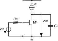
It is sometimes useful to define FoM that are specific to the design of particular analog and RF circuits. If low-power is the objective they often contain the \(G_m/I_D\) and eventually some other FoMs. As an example we will derive another FoM that has been successfully used for the design of low-power RF circuits [15] [16] [17] [8]. We will start from the common-source amplifier shown in Figure 15. The small-signal voltage gain \(A_v\) of this circuit is given by \[\begin{equation} A_v \triangleq \frac{\Delta V_D}{\Delta V_{in}} = - \frac{G_m}{G_{ds}+j\omega\,C_L}. \end{equation}\] If we assume that the transistor needs to drive another stage which has the same input capacitance as the CS source (corresponding to a fan-out of 1) then \(C_L = C_{GS}\). At frequencies higher than the cut-off frequency \(G_{ds}/C_L\) the voltage simplifies to \[\begin{equation} A_v \cong - \frac{G_m}{j\omega C_{GS}} = j \frac{\omega_u}{\omega}, \end{equation}\] with \(\omega_u = G_m/C_L = G_m/C_{GS} \cong \omega_t\). The unity gain frequency then corresponds approximately to the transistor transit frequency.
The noise factor neglecting the contribution from the current source is given by \[\begin{equation}\label{eqn:F_LNA} F = 1 + \frac{\gamma_n}{G_m \cdot R_S}. \end{equation}\]
In a low-noise amplifier (LNA) such as the CS stage shown in Figure 15 we usually want to maximize the \(GBW\) and minimize the noise factor at a given current. To this purpose we can define the following FoM \[\begin{equation}\label{eqn:FoM_LNA} FoM_{LNA} \triangleq \frac{\omega_u}{(F-1) \cdot I_b} \end{equation}\] Introducing \(\eqref{eqn:F_LNA}\) in \(\eqref{eqn:FoM_LNA}\) results in \[\begin{equation} FoM_{LNA} \cong \frac{R_S}{\gamma_n} \cdot \frac{G_m \cdot \omega_t}{I_b}. \end{equation}\] If we ignore the dependence of \(\gamma_n\) to \(IC\), we see that the defined FoM is proportional to \(G_m\,\omega_t/I_D\) which depends on the inversion coefficient and can be defined as the new FoM to be optimized (actually maximized). The normalized \(G_m\,\omega_t/I_D\) can be defined as \[\begin{equation}\label{eqn:FoM_RF} FoM_{RF} \triangleq \frac{g_{ms} \cdot \Omega_t}{IC} \end{equation}\] where \(\Omega_t\) is defined as \[\begin{equation} \Omega_t \triangleq \frac{\omega_t}{\omega_{tspec}} = g_{ms}(IC). \end{equation}\] Replacing \(\Omega_t\) in \(\eqref{eqn:FoM_RF}\) leads to \[\begin{equation}\label{eqn:FoM_RF2} FoM_{RF} = \frac{g_{ms}^2}{IC} = \frac{1}{IC} \cdot \left(\frac{\sqrt{4IC+1+(\lambda_c IC)^2}-1}{2+\lambda_c^2 IC}\right)^2, \end{equation}\] which has the following asymptotes \[\begin{equation}\label{eqn:FoM_RF3} FoM_{RF} \cong \begin{cases} IC & \textsf{WI ($IC \ll 1$)}\\ 1 & \textsf{SI without VS ($IC \gg 1$ and $\lambda_c = 0$)}\\ \frac{1}{\lambda_c^2 \cdot IC} & \textsf{SI with VS ($IC \gg 1$ and $\lambda_c > 0$)}. \end{cases} \end{equation}\] Equation \(\eqref{eqn:FoM_RF2}\) is plotted versus the inversion coefficient in Figure 16.
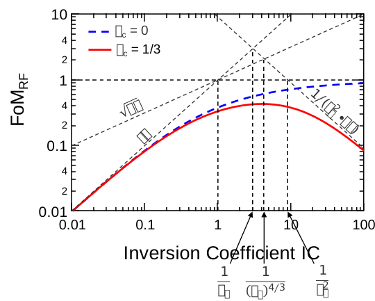
In weak inversion, \(g_{ms} = IC\) and hence \(FoM_{RF} = g_{ms}^2/IC = IC\) with or without velocity saturation. In strong inversion and without velocity saturation, \(g_{ms} = \sqrt{IC}\) and hence \(FoM_{RF}\) tends to unity as shown by the dashed blue line in Figure 16. When velocity saturation is accounted for, \(g_{ms} = 1/\lambda_c\) and hence \(FoM_{RF} = g_{ms}^2/IC = 1/(\lambda_c^2 \cdot IC)\) and scales as \(1/IC\). This means that when velocity saturation is present, \(FoM_{RF}\) reaches a maximum that is located in the moderate inversion region as shown in Figure 16. A good approximation for the optimum \(IC\) at which \(FoM_{RF}\) reaches a maximum is \(IC_{opt} \cong 1/\lambda_c^{4/3}\).
This \(FoM_{RF}\) FoM has been validated on the same 40 and 28 nm bulk technologies. The results are shown in Figure 17 [11].
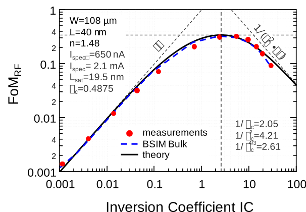
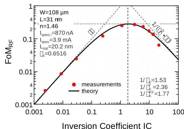
Figure 17 (a) shows the measurements made on on an nMOS transistor from the same 40 nm bulk CMOS technology. We see that the analytical expression \(\eqref{eqn:FoM_RF2}\), which only depends on \(IC\) and the velocity saturation parameter \(\lambda_c\), is fitting the measurements very well despite its simplicity [11]. We also see that the simple analytical expression is close to the BSIM Bulk simulations. The maxium of the RF FoM \(FoM_{RF}\) is reached for \(IC \cong 1/\lambda_c^{4/3} = 2.61\) which is in the moderate inversion region.
Figure 17 (b) shows the FOM \(FoM_{RF}\) measured on an nMOS transistor from the same 28 nm bulk CMOS technology. We again see a very good fit between the simple analytical expression \(\eqref{eqn:FoM_RF2}\) and the measured data [11]. The maximum of \(FoM_{RF}\) is now reached for a slightly smaller inversion coefficient \(IC \cong 1/\lambda_c^{4/3} = 1.77\) almost in the middle of the moderate inversion region.
Since all the FoM \(G_m/I_D\), \(F_t\) and \(G_m/I_D\,F_t\) depend on the same variable \(IC\), they can be plotted together sharing the same x-axis as shown in Figure 18.
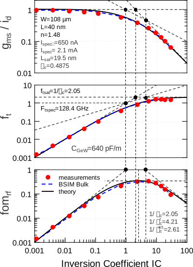
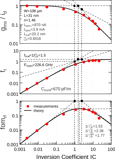
Figure 18 nicely illustrates the trade-off between current efficiency represented by the normalized \(G_m/I_D\) FoM and the unity gain frequency (or gain-bandwidth product) represented by the transit frequency FoM. As we increase the inversion coefficient, we increase the transit frequncy and hence the bandwidth at the cost of a lower current efficiency. The trade-off between the two is represented by \(fom_{rf}\) which turns out ot be in the moderate inversion region.
It is important to mention that, although the \(FoM_{RF}\) FoM gives an optimum inversion coefficient at which \(FoM_{RF}\) reaches a maximum, it does not necessarily mean that all the individual specifications are reached. For example, as shown in [16], the noise figure is rather large. If it was set as a hard specification, the optimum inversion coefficient given by the maximum of \(FoM_{RF}\) would not satistfy a more constraining noise specs.
6.3.4 The input-referred thermal noise resistance
Another important specification that depends directly on the transconductance is the thermal noise. The input-referred thermal noise resistance of a simple CS stage is given by \[\begin{equation} R_{nt} = \frac{\gamma_n}{G_m} \end{equation}\] or in normalized form \[\begin{equation}\label{eqn:rn_def} r_{nt} \triangleq G_{spec} \cdot R_{nt} = \frac{\gamma_n}{g_m} \end{equation}\] where \(\gamma_n\) is the thermal noise excess factor. For a long-channel transistor in saturation, the thermal noise excess factor \(\gamma_n\) is given by \[\begin{equation} \gamma_n \cong \begin{cases} \frac{n}{2} & \textsf{WI}\\ \frac{2}{3} \cdot n & \textsf{SI}. \end{cases} \end{equation}\]
In RF circuit we often need to choose the minimum length and the we cannot ignore the effect of velocity saturation on the transconductance \(G_m\) but also on the thermal noise excess factor \(\gamma_n\) as shown by the measurements of \(\gamma_n\) versus \(IC\) shown in Figure 19.
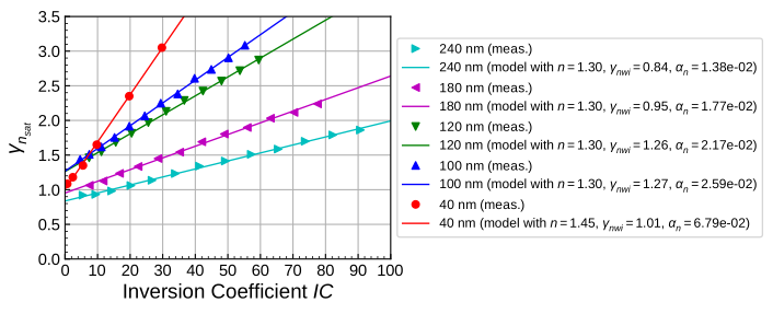
Figure 19 shows that \(\gamma_n\) increases about lineraly from its value in weak inversion. The slope is steeper as the technology is more advanced. \(\gamma_n\) can be modeled by the empirical model given by \[\begin{equation} \gamma_n = \gamma_{nwi} + \alpha_n \cdot IC,\label{eqn:gamman_ic} \end{equation}\] where \(\gamma_{nwi}\) is the value of \(\gamma_n\) in weak inversion and parameter \(\alpha_n\) depends \(\lambda_c\) according to \[\begin{equation} \alpha_n = \frac{n}{2} \cdot \lambda_c^2. \end{equation}\] Theoretically \(\gamma_{nwi} \cong n/2\) and \(\alpha_n = n/2 \cdot \lambda_c^2\), but as shown in Figure 19, the values extracted from experimental data are closer to 1. \(\gamma_{nwi}\) is therefore used as a fitting parameter which is usually close to 1.
In weak inversion, \(\gamma_n = \gamma_{nwi}\) and \(g_m \cong IC/n\), results in \[\begin{equation} r_{nt,wi} \cong \frac{n \cdot \gamma_{nwi}}{IC} \propto \frac{1}{IC}, \end{equation}\] which is inversely proportional to \(IC\). In strong inversion, we have \(\gamma_n \cong \alpha_n \cdot IC\) and \(g_m \cong 1/(n \lambda_c)\) resulting in \[\begin{equation} r_{nt,si} \cong \alpha_n \cdot \lambda_c \cdot n \cdot IC = \frac{n^2}{2} \cdot \lambda_c^3 \cdot IC \propto IC \end{equation}\] which is proportional to \(IC\). \(r_{nt}\) should therefore reach a minimum in terms of \(IC\). The optimum \(IC\) corresponding to the minimum \(r_{nt}\) can be approximated by equating \(r_{nt,wi}\) and \(r_{nt,si}\) and solving for \(IC\) resulting in \[\begin{equation} IC_{opt} \cong \sqrt{\frac{\gamma_{nwi}}{\alpha_n \cdot \lambda_c}} = \sqrt{\frac{2 \gamma_{nwi}}{n \cdot \lambda_c^3}}. \end{equation}\] The normalized input-referred thermal noise resistance \(r_{nt}\) is plotted versus the inversion coefficient \(IC\) in Figure 20 which shows a minimum in the upper side of moderate inversion with \(r_{nt} \cong 1.178\) for \(IC_{opt} \cong 8.913\).
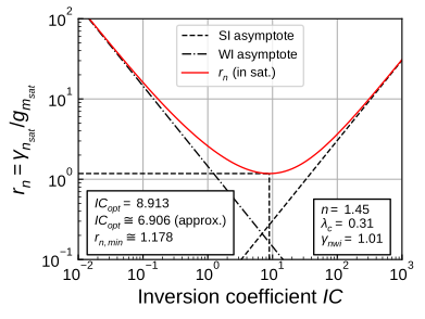
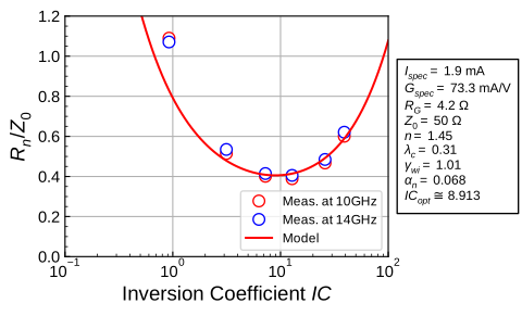
Note that this minimum of \(\gamma_n/G_m\) is important when optimizing RF circuits such as low-noise amplifiers (LNAs). The input-referred noise resistance for a CS stage at RF is given by \[\begin{equation} R_n \cong \frac{\gamma_n}{G_m} + R_G, \end{equation}\] where the gate resistance \(R_G\) directly adds to \(R_n\). This input-referred noise resistance has been measured for a nMOS transistor from 40 nm bulk CMOS at two different RF frequencies of 10 and 14 GHz. The measured values normalized to \(50\,\Omega\) are plotted versus the inversion coefficient \(IC\) in Figure 21 and compared to the result of the above model for the two measurement frequencies. The minimum of the input-referred noise resistance \(R_n\) occurs on the upper side of the moderate inversion at about \(IC_{opt} \cong 10\). We see a good match between the model and the measurements in the region of the minimum input-referred thermal noise resistance. This means that the simple model versus \(IC\) presented above can capture the optimum inversion coefficient \(IC_{opt}\) to minimize the input-referred noise resistance \(R_n\).
6.3.5 The minimum noise factor
Another FoM that is used in RF design is the minimum noise factor \(F_{min}\) or minimum noise figure \(NF_{min}=10\,\log(F_{min})\). \(F_{min}\) represents the minimum noise factor (figure) that can be achieved at a given operating point under noise impedance matching conditions [9]. It can be shown that the actual noise factor of a CS transistor is given by [18] [9] \[\begin{equation} F = F_{min} + \frac{R_n}{G_s} \cdot \left[(G_s-G_{opt})^2 + ( B_s-B_{opt})^2\right], \end{equation}\] where \(G_s \triangleq \Re\{Y_s\}\) and \(B_s \triangleq \Im\{Y_s\}\) are the real and imaginary parts of the source admittance \(Y_s\). The noise factor is then characterised by four noise parameters, namely the minimum noise factor \(F_{min}\), the input-referred noise resistance \(R_n\) (which is discussed in the previous Section), the optimum source conductance \(G_{opt}\) and susceptance \(B_{opt}\). The noise factor reaches the minimum noise factor \(F_{min}\) for \(G_s=G_{opt}\) and \(B_s=B_{opt}\). This condition corresponds to noise matching which in general is different from the impedance matching condition required to transfer a maximum of power from the source to the load (the transistor input in this case).
It can be shown that the minimum noise factor is approximately given by [18] [9] \[\begin{equation}\label{eqn:Fmin_IC} F_{min} \cong 1 + 2\omega C_{GS} \cdot \frac{\gamma_n}{G_m} \cdot \sqrt{\alpha_G + b_n}, \end{equation}\] where \(b_n \cong 2/(5 n^2)\) and \(\alpha_G\) is the thermal noise contribution of the gate resistance normalized to that of the channel \[\begin{equation} \alpha_G \triangleq \frac{G_m \cdot R_n}{\gamma_n}. \end{equation}\]
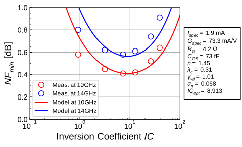
The minimum noise figure has been measured at different bias currents and at two frequencies 10 GHz and 14 GHz on a CS transistor with minimum length from a 40 nm bulk CMOS technology. The measurements are shown in Figure 22 and compared to the results obtained using \(\eqref{eqn:Fmin_IC}\). We see a minimum of the minimum noise figure that occurs about at the same inversion coefficient than the minimum of the input-referred noise resistance \(R_n\) presented in the previous Section. Again, we can observe a very good match between the measurements and the simple model particularly in the region of the minimum. The simple model proposed above can therefore predict the optimum inversion coefficient \(IC_{opt}\) for which the minimum noise figure reaches a minimum.
6.3.6 The Fano noise suppression factor
The Fano noise suppression factor \(F_a\) was introduced in the modeling chapter ???. It is defined as the ratio of the actual PSD of the white noise fluctuations in the drain current to the shot noise \(2 q I_D\) corresponding to the DC current \[\begin{equation}\label{eqn:Fa_IC} F_a \triangleq \frac{S_{\Delta I_D^2}}{2 q I_D} = \frac{4 k_B\,T\,\gamma_n\,G_m}{2 q I_D} = \frac{2}{n} \cdot \gamma_n(IC) \cdot \frac{g_{ms}(IC)}{IC}. \end{equation}\] From \(\eqref{eqn:Fa_IC}\), we see that the Fano noise suppression factor is proportional to the product of the normalized \(G_m/I_D\) ratio and the thermal noise excess factor. For short-channel transistors we need to account for the dependence of \(\gamma_n\) on \(IC\) \[\begin{equation} \gamma_n = \gamma_{nwi} + \alpha_n \cdot IC, \end{equation}\] with \(\gamma_{nwi} = n/2\) and \(n/2 \cdot \lambda_c^2\). Replacing in \(\eqref{eqn:Fa_IC}\) results in \[\begin{equation} F_a = (1 + \lambda_c^2 \cdot IC) \cdot \frac{g_{ms}(IC)}{IC} \cong \begin{cases} 1 & \textsf{WI ($IC \ll 1$)}\\ \lambda_c & \textsf{SI with VS ($IC \gg 1$ and $\lambda_c > 0$)}. \end{cases} \end{equation}\] \(F_a\) is plotted in Figure 23 versus \(IC\) for various \(\lambda_c\).
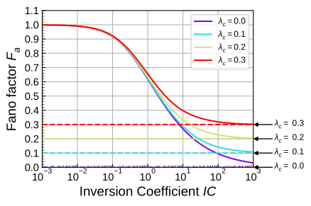
In weak inversion, \(F_a \cong 1\), whereas in strong inversion, \(F_a \cong \lambda_c\). This means that there is less noise suppression in strong inversion for a short-channel transistor compared to a long-channel transistor because of velocity saturation. This also means that in strong inversion under heavy velocity saturation, the PSD of the drain current fluctuations can be considered as shot noise with \[\begin{equation} S_{\Delta I_D^2} = \lambda_c \cdot 2 q I_D. \end{equation}\]
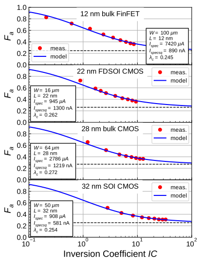
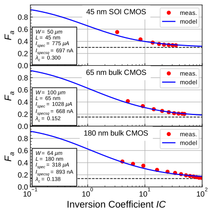
The theoretical expression of the Fano noise factor given by \(\eqref{eqn:Fa_IC}\) is compared to measurements made by Das on several technologies ranging from 180 nm down to 12 nm [20]. Notice how the measurements points move progressively from strong inversion to moderate inversion. This is due to voltage scaling which pushes the operating points towards moderate inversion.
This shows that the white noise PSD of the drain current fluctuations can be estimated using the Fano noise suppression factor given by \(\eqref{eqn:Fa_IC}\) and the bias current \(I_D\) \[\begin{equation} S_{\Delta I_D^2} = F_a(IC) \cdot 2 q I_D. \end{equation}\]